ones aldeT rihnT olgmo3 ngleed oorpo ovengnohow eono S baupen o barlainit uoy to Noy adeitenome of fuio prhow holsH S his lsfipib A PRINČI 2-2) Obtain a simplitied Boolean outpuưt function Ffx V. z) using the k-map method. Show your work using the blank map given below: Truth 23. 16/7 4/5 Demon F(x, y, z) = 2-3) In the space below, draw a schematic diagram of F(x, y, z) found above using NAND gates with a minimum number of ICs (an IC diagram is optional). Label everything on your diagram (IC and pin numbers, switch numbers, indicator lamp numbers, etc.). Your diagrams should include enough information so that anyone unfamiliar with the process above could still build it. (Hint: you will need two different ICs.) Schematic Diagram: ablo Even Pe (expecied) of 98ur work using the blank map given below: 'pounau deu Dun BD BC 1213 14 AB l8|1911110 F(A, B, C, D) = AB+ Bct BD 1-3) In the space below, draw a circuit logic diagram of F(A, B, C, D) found above using NAND gates with a minimum number of ICs (an IC diagram is optional). Label everything on each diagram (IC and pin numbers, switch numbers, indicator lamp numbers, etc.). Your diagrams should include enough information so that anyone unfamiliar with the process above could still build it. (Hint: you will need two different ICs.) AB+BCHBN Schematic:
ones aldeT rihnT olgmo3 ngleed oorpo ovengnohow eono S baupen o barlainit uoy to Noy adeitenome of fuio prhow holsH S his lsfipib A PRINČI 2-2) Obtain a simplitied Boolean outpuưt function Ffx V. z) using the k-map method. Show your work using the blank map given below: Truth 23. 16/7 4/5 Demon F(x, y, z) = 2-3) In the space below, draw a schematic diagram of F(x, y, z) found above using NAND gates with a minimum number of ICs (an IC diagram is optional). Label everything on your diagram (IC and pin numbers, switch numbers, indicator lamp numbers, etc.). Your diagrams should include enough information so that anyone unfamiliar with the process above could still build it. (Hint: you will need two different ICs.) Schematic Diagram: ablo Even Pe (expecied) of 98ur work using the blank map given below: 'pounau deu Dun BD BC 1213 14 AB l8|1911110 F(A, B, C, D) = AB+ Bct BD 1-3) In the space below, draw a circuit logic diagram of F(A, B, C, D) found above using NAND gates with a minimum number of ICs (an IC diagram is optional). Label everything on each diagram (IC and pin numbers, switch numbers, indicator lamp numbers, etc.). Your diagrams should include enough information so that anyone unfamiliar with the process above could still build it. (Hint: you will need two different ICs.) AB+BCHBN Schematic:

COMPREHENSIVE MICROSOFT OFFICE 365 EXCE
1st Edition
ISBN:9780357392676
Author:FREUND, Steven
Publisher:FREUND, Steven
Chapter6: Creating, Sorting, And Querying A Table
Section: Chapter Questions
Problem 10EYK

Related questions

Question
How do i draw these schematics

Transcribed Image Text:ones
aldeT rihnT olgmo3 ngleed
oorpo ovengnohow eono
S baupen o barlainit uoy to
Noy adeitenome
of fuio prhow
holsH S his
lsfipib A
PRINČI
2-2) Obtain a simplitied Boolean outpuưt function Ffx V. z) using the k-map method. Show
your work using the blank map given below:
Truth
23.
16/7
4/5
Demon
F(x, y, z) =
2-3) In the space below, draw a schematic diagram of F(x, y, z) found above using NAND
gates with a minimum number of ICs (an IC diagram is optional). Label everything on
your diagram (IC and pin numbers, switch numbers, indicator lamp numbers, etc.). Your
diagrams should include enough information so that anyone unfamiliar with the process
above could still build it. (Hint: you will need two different ICs.)
Schematic Diagram:
ablo
Even
Pe
(expecied)

Transcribed Image Text:of
98ur work using the blank map given below:
'pounau deu Dun
BD
BC
1213
14
AB
l8|1911110
F(A, B, C, D) = AB+ Bct BD
1-3) In the space below, draw a circuit logic diagram of F(A, B, C, D) found above using
NAND gates with a minimum number of ICs (an IC diagram is optional). Label everything
on each diagram (IC and pin numbers, switch numbers, indicator lamp numbers, etc.).
Your diagrams should include enough information so that anyone unfamiliar with the
process above could still build it. (Hint: you will need two different ICs.) AB+BCHBN
Schematic:
Expert Solution
Step 1
The final output of the K-map F(x, y, z) = xyz + z
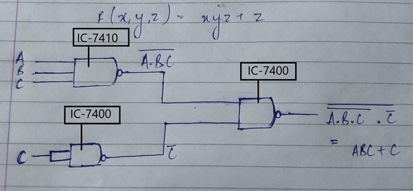
The IC-7410 is a NAND gate IC and is used to accept three inputs.
The IC-7400 is also a NAND gate IC and is used to accept two inputs.

Step by step
Solved in 2 steps with 2 images

Knowledge Booster


Learn more about
Need a deep-dive on the concept behind this application? Look no further. Learn more about this topic, computer-science and related others by exploring similar questions and additional content below.Recommended textbooks for you
COMPREHENSIVE MICROSOFT OFFICE 365 EXCE
Computer Science
ISBN:
9780357392676
Author:
FREUND, Steven
Publisher:
CENGAGE L
COMPREHENSIVE MICROSOFT OFFICE 365 EXCE
Computer Science
ISBN:
9780357392676
Author:
FREUND, Steven
Publisher:
CENGAGE L