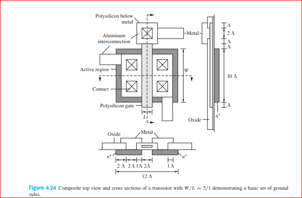
Polysilicon below metal -Metal- Aluminum interconnection Active region 10 A Contact Polysilicon gate Oxide Metal Oxide ele+He-| 2A 2A 1A 2A 1A 12 A Figure 4.24 Composite top view and cross sections of a transistor with W/L = 5/1 demonstrating a basic set of ground rules.
Polysilicon below metal -Metal- Aluminum interconnection Active region 10 A Contact Polysilicon gate Oxide Metal Oxide ele+He-| 2A 2A 1A 2A 1A 12 A Figure 4.24 Composite top view and cross sections of a transistor with W/L = 5/1 demonstrating a basic set of ground rules.

Related questions
Question
What is the active area of the transistor if ∆ = 0.125 μm? What
are the values of W and L for the transistor. What is the area of the transistor gate region?
How many of these transistors could be packed together on a 10 mm × 10 mm integrated
circuit die if the active areas of the individual transistors must be spaced apart by a minimum
of 4 ∆?
Transcribed Image Text:Polysilicon below
metal
-Metal-
Aluminum
interconnection
Active region
10 A
Contact
Polysilicon gate
Oxide
Metal
Oxide
ele+He-|
2A 2A 1A 2A
1A
12 A
Figure 4.24 Composite top view and cross sections of a transistor with W/L = 5/1 demonstrating a basic set of ground
rules.
Expert Solution
Step 1
Given:
Step 2
Concept:
The part of the chip at the top in which all the actions of the chip takes place is called as active area. It consists of transistors and resistors.
Step 3
Formula used:

Step by step
Solved in 5 steps with 11 images
