Q1.31 The circuit diagram for the following Verilog statement is: timescale 1 ns /1 ps // time units / resolution module and_or_prop_delay( input A, B, C, D; Output D, E; wire w1; and G1 #30 (w1 A, B); //Prop delay: 30 ns not G2 #10 (E, C): //Prop delay: 10 ns or G3 #20 (D, w1, E); //Prop delay: 20 ns endmodule GI Your answer: O Yes O No
Q1.31 The circuit diagram for the following Verilog statement is: timescale 1 ns /1 ps // time units / resolution module and_or_prop_delay( input A, B, C, D; Output D, E; wire w1; and G1 #30 (w1 A, B); //Prop delay: 30 ns not G2 #10 (E, C): //Prop delay: 10 ns or G3 #20 (D, w1, E); //Prop delay: 20 ns endmodule GI Your answer: O Yes O No
C++ for Engineers and Scientists
4th Edition
ISBN:9781133187844
Author:Bronson, Gary J.
Publisher:Bronson, Gary J.
Chapter1: Fundamentals Of C++ Programming
Section1.3: Preliminary Three: Software Development
Problem 3E: (Electrical eng.) You’ve been asked to write a program that outputs the following specifications:...

Related questions
Question
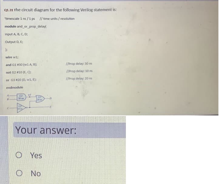
Transcribed Image Text:Q1.31 The circuit diagram for the following Verilog statement is:
"timescale 1 ns /1 ps // time units / resolution
module and_or_prop_delay(
input A, B, C, D;
Output D, E;
wire w1;
and G1 #30 (w1 A, B);
//Prop delay: 30 ns
not G2 #10 (E, C);
//Prop delay: 10 ns
or G3 #20 (D, w1, E);
//Prop delay: 20 ns
endmodule
w/
GI
30 ms
Your answer:
O Yes
O No
Expert Solution
This question has been solved!
Explore an expertly crafted, step-by-step solution for a thorough understanding of key concepts.

This is a popular solution!

Trending now
This is a popular solution!

Step by step
Solved in 2 steps

Knowledge Booster


Learn more about
Need a deep-dive on the concept behind this application? Look no further. Learn more about this topic, computer-science and related others by exploring similar questions and additional content below.Recommended textbooks for you
C++ for Engineers and Scientists
Computer Science
ISBN:
9781133187844
Author:
Bronson, Gary J.
Publisher:
Course Technology Ptr
C++ for Engineers and Scientists
Computer Science
ISBN:
9781133187844
Author:
Bronson, Gary J.
Publisher:
Course Technology Ptr