Simplity the following expressions using Boolean algebra. (a) x- ABC+ AC (b) y= (0+ AX+ R) () ABC+ ABC+ A
Simplity the following expressions using Boolean algebra. (a) x- ABC+ AC (b) y= (0+ AX+ R) () ABC+ ABC+ A

Introductory Circuit Analysis (13th Edition)
13th Edition
ISBN:9780133923605
Author:Robert L. Boylestad
Publisher:Robert L. Boylestad
Chapter1: Introduction
Section: Chapter Questions
Problem 1P: Visit your local library (at school or home) and describe the extent to which it provides literature...

Related questions
Question
100%
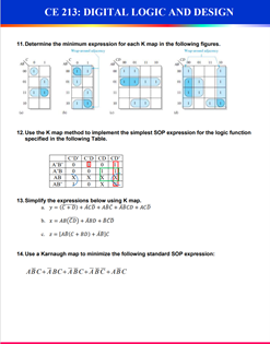
Transcribed Image Text:CE 213: DIGITAL LOGIC AND DESIGN
11. Determine the minimum epresion for each Kmap in the following figures.
12. Use the Kmag method to implement the simplest SOP pression for the logic function
specified in the following Table.
AB
13. Simpity e epressions below using Kmap.
14 Use a Karnaugh map to minimiae the tolilowing standard soPpression
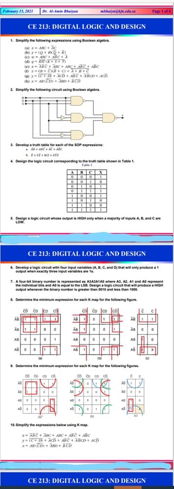
Transcribed Image Text:February 15, 202I
Dr. Al-Amin hwiyan
mbhwiywa kfu.edu. sa
Page I of 4
CE 213: DIGITAL LOGIC AND DESIGN
1. Simplify the following expressions using Boolean algebra
(a) x- ABC + AC
(b) y= (Q+ KXQ+R)
(C) - ABc+ AliC + A
(d) g k OR+S+D
(e) x- ABC + AnC + ABC+ ARC + AHC
() y- tC+ + ACD + ABC + ABCD+ ACD
(h) x AB (CD) + AND + BCD
2. Simplify the following circuit using Boolean algebra.
3. Develop a truth table for each of the SOP expressions:
a A ABC + AC + ABC
4. Design the logic circuit corresponding to the truth table shown in Table 1
Table I
ABI CX
0
5. Design a logic circuit whose output is HIGH only when a majority of inputs A, B, and C are
LOW.
CE 213: DIGITAL LOGIC AND DESIGN
6. Develop a logic circuit with four input variables (A B. C, and D) that willl only produce a1
output when exactly three input variables are 1s.
7. A four-bit binary number is represented as AJAZA1A0 where A3, A2, A1 and AO represent
the individual bits and AO is equal to the LSB. Design a logic circuit that will produce a HIGH
output whenever the binary number is greater than 0010 and less than 1000.
8. Determine the minimum expression for each K map for the following figure.
čo čo co că
čo čo |co Jcol
AB IO
ÄB 0
AB O00 0
AB
AB
la
(bi
9. Determine the minimum expression for each K map for the following figures.
Co čo co co
AB
Co Co co co
AB
ele
ABO
AB
A
AB
(b)
10. Simplify the expressions below using Kmap
x- ABC + ABC + ABC + ABT + AĒC
y- (C+ D + ACD+ ANC + ABCD + ACD
x- AB CD) + AnD + BED
CE 213: DIGITAL LOGIC AND DESIGN
Expert Solution
This question has been solved!
Explore an expertly crafted, step-by-step solution for a thorough understanding of key concepts.

Step by step
Solved in 2 steps with 2 images

Knowledge Booster


Learn more about
Need a deep-dive on the concept behind this application? Look no further. Learn more about this topic, electrical-engineering and related others by exploring similar questions and additional content below.Recommended textbooks for you
Introductory Circuit Analysis (13th Edition)
Electrical Engineering
ISBN:
9780133923605
Author:
Robert L. Boylestad
Publisher:
PEARSON

Delmar's Standard Textbook Of Electricity
Electrical Engineering
ISBN:
9781337900348
Author:
Stephen L. Herman
Publisher:
Cengage Learning

Programmable Logic Controllers
Electrical Engineering
ISBN:
9780073373843
Author:
Frank D. Petruzella
Publisher:
McGraw-Hill Education
Introductory Circuit Analysis (13th Edition)
Electrical Engineering
ISBN:
9780133923605
Author:
Robert L. Boylestad
Publisher:
PEARSON
Delmar's Standard Textbook Of Electricity
Electrical Engineering
ISBN:
9781337900348
Author:
Stephen L. Herman
Publisher:
Cengage Learning
Programmable Logic Controllers
Electrical Engineering
ISBN:
9780073373843
Author:
Frank D. Petruzella
Publisher:
McGraw-Hill Education

Fundamentals of Electric Circuits
Electrical Engineering
ISBN:
9780078028229
Author:
Charles K Alexander, Matthew Sadiku
Publisher:
McGraw-Hill Education

Electric Circuits. (11th Edition)
Electrical Engineering
ISBN:
9780134746968
Author:
James W. Nilsson, Susan Riedel
Publisher:
PEARSON

Engineering Electromagnetics
Electrical Engineering
ISBN:
9780078028151
Author:
Hayt, William H. (william Hart), Jr, BUCK, John A.
Publisher:
Mcgraw-hill Education,