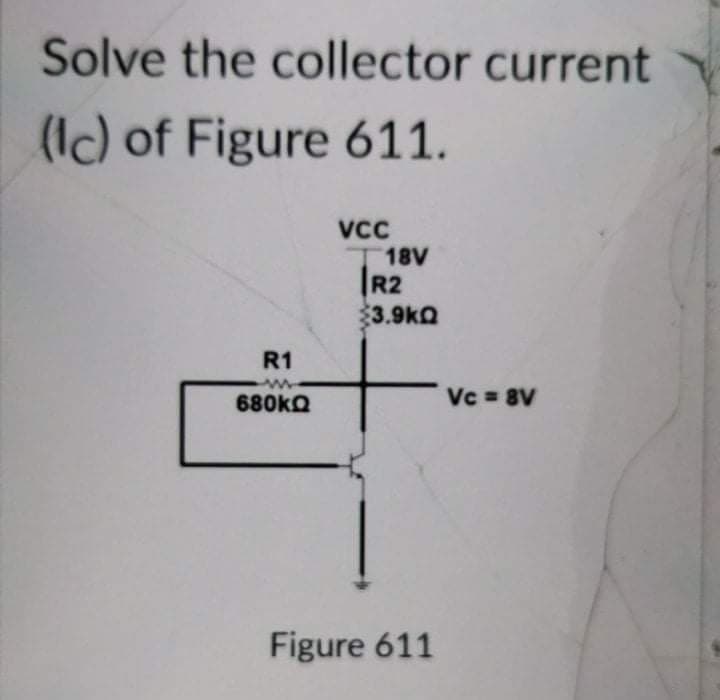
Solve the collector current (Ic) of Figure 611. VC T18V R2 3.9ka R1 680ko Vc 8V Figure 611


Q: Figure 2 (for numbers 10 to 14). Vcc= 6V, RB =10k, RC=1k, B(beta)=100, hie=1k. Vcc O Vo A V₁O Zo'…
A: Given data Vcc=6V Rb=10k Rc=1k Beta=100
Q: Q1: Verify the mode of operation with justification and draw the load line for each transistor shown…
A: Steps to find the Mode of operation of the transistor Convert AC equivalent model into DC Model by…
Q: Calculate Ic(sat) CE EMITTER-BIAS CONFIGURATION 0 22 V 3,3 kQ 330 k2 I, Cc V; 0 Cc B= 80 Z; 1.2 k2…
A: Brief description: For the given common emitter emitter bias configuration we need to calculate its…
Q: 4 bit R-2R Digital Analog Converter is also applied as reference voltage +5V. Accordingly, in which…
A: A combinational circuit is one in which the various gates in the circuit, such as the encoder,…
Q: Complete the sentence: Based from Bell Telephone Laboratories, transistor is an abbreviated…
A: In this question we will answer about BJT related questions...
Q: Q1: find the emitter, base and collector currents and Vt. (let any parameters if you need). • Vec6V…
A: Apply Kirchhoff's voltage law at input and assume VBE =0.7V side we get Now apply KVL at output…
Q: The current gain α of a transistor is 0.995. If the change in emitter current is 10 mA, the change…
A:
Q: For a certain transistor, IC = 5.505 mA, IB = %3D %3D 50 mA, ICO = 5 mA. Determine (i) values of a,…
A: Since we are allowed to solve only first question the solution below contains answer for the first…
Q: Voltage applied to the Anode of the CRT is less than the voltage applied Select one: O True O False
A: CRT-It is known as the cathode ray tube. It produces images on the striking of electrons.
Q: Q3 Determine the RB whicheJllI make the transistor work as ON-OFF switch if you knew value of the…
A:
Q: When a p-type material is sandwiched between two n-type materials such type of transistor is called:…
A:
Q: 1863 224 2,525 10 ㅛ ft IDB-SmA Up=-60 2U R₂ 1k If VCE is SV in the circuits and green led is on,…
A:
Q: In the transistor shown below choose the correct terminal names Terminal 1 Terminal 2 o- Terminal 3…
A: As arrow mark is inward it is a PNP transistor. Arrow mark always indicated at emitter. Opposite…
Q: 0.605 REB > Rce 0.6 17 E B Figure-7e IDENTIFIED AS PNP Table 7-b: PNP Transistor Meter Leads Step…
A: A transistor is a semiconductor device constructed by sandwiching three n-p-n or p-n-p layers that…
Q: Assuming a JFET has an Ipss = 5 mA and VGs(off) = -7 V (maximum). Using these values, determine the…
A: By drain current equation we will find out drain current.
Q: a. all transistor terminal voltages with respect to ground b. currents Ic. Ig and Ig +9 V Rc 2.2 kN…
A: All transistor terminal voltages with respect to ground Base resistance…
Q: A unjunchion transistor has lov intrinsie ctand aff ratio is 0.45· find the value a stand hetween…
A:
Q: Calculate iT for an npn transistor with IS = 10−15 μAfor (a) VB E = 0.70 V and VBC = −3 V and(b) VBC…
A: Given: IS=10-15 AVBE=0.70 V & -3.0 VVBC=-3.0 V & 0.70 V
Q: 1. Determine IB, Ic, IE, VBE, VCE, and VCB in the circuit shown in FigureA1. The [2M] transistor has…
A: The solution is given below
Q: Rc 1.5 k + Ve15 V Boc= 100 Van= 4.0 VE BB The largest base resistor that will still saturate the…
A:
Q: Vcc For the shown sillicon transistor of B=70, Rc assume that V=18 V, CC R=370 KO, VE R=2 KQand R=11…
A: To find the base Current IBQ for the given BJT circuit
Q: For the FET transistor circuit in Figure 1, a) Determine: i. voltage, VGso ii. current, Ipo iii.…
A: As per company guidelines we can solve only first three sub parts kindly post another parts…
Q: In the transistor shown below choose the correct terminal names Terminal 1 Terminal 2 o- Terminal 3…
A: BJT containe three terminals, namely Collector Emitter Base
Q: QUESTION 2 Refer to Figure 3 and answer the following questions: (i) Calculate the minimum value of…
A:
Q: transistor has the CB input characteristics shown in Figure 3–11 (p. 106 ). If alpha = 0.95, find…
A:
Q: An NPN transistor with ICRO=0.5µA ICEO=45 µA and collector current СВО СЕО 2mA. Calculate the value…
A:
Q: 5- Describe abbreviate the function of each block shown below: Scope Mux Product
A: There are various blocks which can be used in matlab simulink for the simulation of particular…
Q: In an NPN transistor 108 electrons enter the emitter in 10–8 s. If 1% electrons are lost in the…
A: Given, NPN transistor having Number of electrons enter the emitter (Ne) = 108 in 10-8 Seconds…
Q: Q: For the transistor shown below, determine (a) IBo and Ico (b) VCEQ (c) Va and Ve (d) VBc (e)…
A: Do DC analysis, remove the capacitor. Let's assume the BJT is in the active region. And the voltage…
Q: +18 V 18 k2 18 k2 Vi2 Vis 8=200 2 mA -18 V
A: The problem is from biasing of BJT.
Q: 12V Rc 7502 Vin = 5v Ov Q1 50kO 2SC2001 Rb
A: BJT is a current controlled Device in which base current control the mode of operation of BJT Model…
Q: Calculate iT for an npn transistor with IS = 10−16 μAfor (a) VB E = 0.75 V and VBC = −3 V and(b) VBC…
A: (a) Given Saturation current IS=10-16 A Base-emitter voltage VBE=0.75 V Base collector voltage…
Q: +18 V Si transistor; B=50 Determine: g) dc transistor terminal voltages h) hie i) Ri i) v. k) Ais…
A:
Q: In Figure 2.2 is shown the fixed bias circuit of a Silicon transistor with B = 180. Determine the…
A: We need to find out unknown resistance value for given circuit
Q: What is the current gain for a common-base configuration where IE = 4.2mA and IC = 4.0 ?mA c) 16.80…
A:
Q: Determine the Q point of the transistor circuit shown in Figure. Given B= 200 and VBE = 0.7V. 33092…
A:
Q: nswer with (V) or (X) and correct of the followings: a) Thyristor can be used as a switch and as…
A: As per Bartleby guidelines we are allowed to solve only first three subparts, please ask the rest…
Q: Q6:A) A transistor dissipates 50W in an ambient temperature of 60°C.The thermal resistance are…
A: The circuit diagram of transistor heating and cooling is where, Pavg =average rate of…
Q: For the transistor shown in below figure, Calculate the value of Rg that will just make the…
A:
Q: QUESTION 3: Refer to the following figure. The circuit parameters are: V*= 4.5 V, V = -4.5 V and R1…
A: The transistor is a three-terminal device used for the regulation of signals. It is used for…
Q: Q4: The input voltage must overcome the junction voltage between the gate and cathode (0.7V) and…
A:
Q: Determine all current and voltage values exactly even if any transistor is on. saturation. R1=7k…
A:
Q: Il-(a) State the fundamental operating principle of the field-effect transistor as a switch.
A: “Since you have asked multiple questions, we will solve the first question for you. If you want any…
Q: For the emitter bias network of Figure 3, determine: (a) IB. (b) lc. (c) VCE. (d) Vc. (e) Ve. (f)…
A: A bipolar junction transistor (BJT) is a three-terminal device with the base as the controlling…
Q: &.9(10%) Each transistor has B=50 Gain = U0/Uin 2kn 2kn RE RE TI 12kr = 25 Maximum output yoltage,…
A: Given: Single input balanced output differential amplifier with constant current bias:…
Q: What is the current gain for a common-base configuration where IE = 4.2 mA and IC = 4.0 mA? * 0.95…
A:
Q: hese are the features of transistors, EXCEPT. O Cheaper Smaller Made of metal plates Dissipates less…
A: Bartleby has policy to solve only one question. Please reupload another question.
Q: Types of MOSTFET transistor are depending on OThe nature of the bulk semiconductor. OThe name of…
A: MOSFET can be classification based on the construction and the material used in it. MOSFETs are of…
Q: For the network of Figure 04, determine the collector-emitter voltage difference VCE And collector…
A: Bias circuit The transistor is a current controlled device and it requires biasing circuit to…

Step by step
Solved in 3 steps


- What is the collector-emitter voltage for thetransistor if IS = 7 × 10⁻¹⁶ μA,αF = 0.99, and αR = 0.5? (b) What is the emittercollector voltage for the transistor P5.56(b)for the same transistor parameters?The dc load line on a family of collector characteristic curves of transistor shows the........ Choose correct answer : A) All operating regions B) cut-off region only C) active region only D) saturation region onlyRb=1Mohm Rc=4.7Kohm VCC=7volt BSX 46 transıstor a)find the dc analysis? b)replace the transistor with 2n2222 and null the Ic and Vc values for the same Vcc value?
- Draw an NPN transistor Circuit with Vbb = 3V, Rb = 23k Ohms, Vcc = 10 V, Rc = 800 Ohms, Beta = 30. Determine Loadline, Vce = ?, Ic =?, mkde of operation. Please show all work. I will definately rate. Thank you!Round off to two decimal points and box the final answer. 1.Draw the DC equivalent circuit. 2.Draw the fixed bias base emitter circuit. Derive IB.3.Draw fixed bias collector emitter loop. Derive VCE.4.Solve for unknowns.15/ In a transistor, _____________________________________________ is the process of making proper flow of zero signal collector current and the maintenance of proper collector-emitter voltage during the passage of signal. a. DC load line drawing b. amplification c. transistor biasing d. stabilization
- Determine the output currents and voltage of the Transistor Ic, IB, VCE. Beta= 120, Vbe = 0.7v.When IB=30uA, Calculate; a.) IE b.) What is the DC gain or beta of the transistor? c.) Calculate the collector current, IC d.) Calculate the VCC for the system. e.) VB f.) What is the proper value of RBDetermine the output voltage of 8-bit successive approximation digitalvoltmeter, if (8V) is the input voltage and (10V) is the reference voltage.
- Sketch the transfer and drain curve characteristics for an n – channel JFET defined by IDSS = 12 mA and VP = – 6 V.draw a qpsk modulator circuit using different circuit compents like resistors, transistors etc not a block diagramI need answer ASAP. Thank you! Given: RD = 2kohm , Rs = 0.51kohm , RG = 1Mohm and VDD = 18V Gate junction saturation current= 6 mA and VTO = -4 V A.) Find the value of drain current and gate current. B.) What type of JFET DC biasing is this? C.) Find the Drain voltage, Emitter Voltage and Gate Voltage.