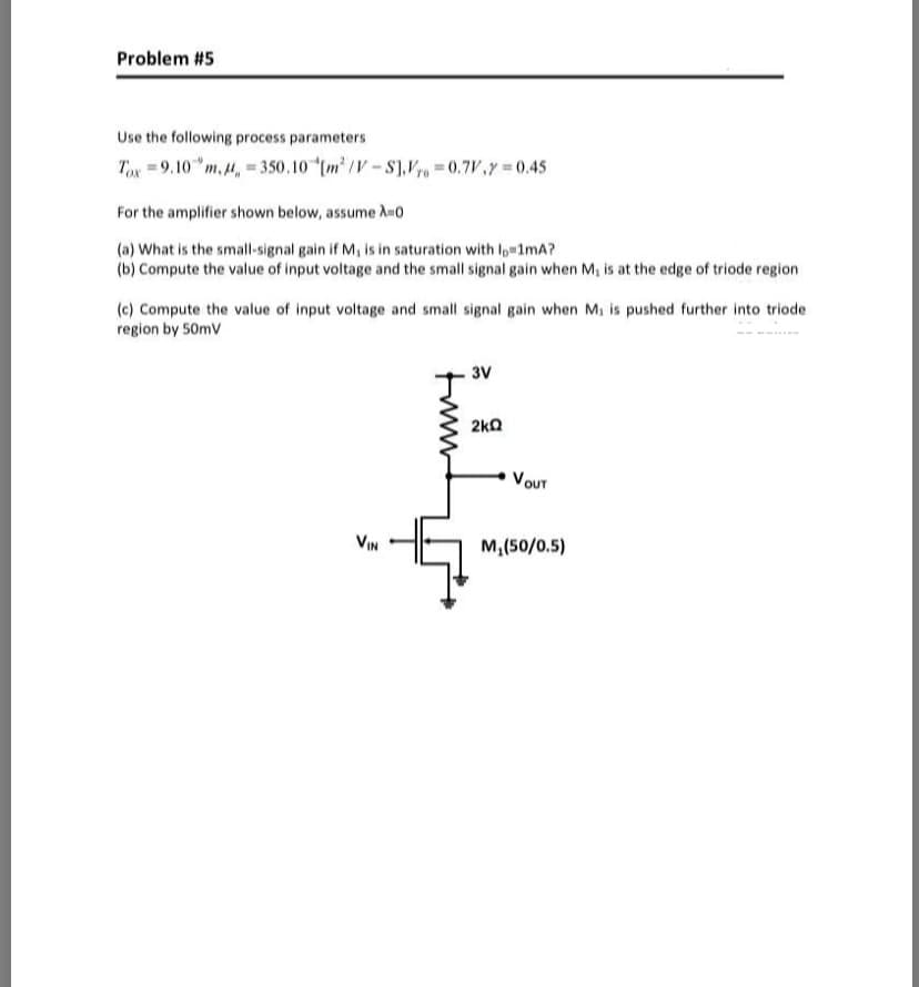
Use the following process parameters Tox =9.10"m, 4, = 350.10 "(m /V-S],Vr = 0.7V,7 0.45 For the amplifier shown below, assume Au0 (a) What is the small-signal gain if M, is in saturation with lo=1lmA? (b) Compute the value of input voltage and the small signal gain when M, is at the edge of triode region (c) Compute the value of input voltage and small signal gain when M, is pushed further into triode region by 50mv
Q: The given circuit is a 2N4403 PNP common collector amplifier. Let VCC=12V, VEE=-12V, R1=52.5kΩ,…
A: The given circuit is a 2N4403 PNP common collector amplifier as shown below: Let VCC=12V, VEE=-12V,…
Q: In the push-pull stage given (in the photo attached), IS1 = 5 × 10⁻¹⁷ A and IS2 = 8 × 10⁻¹⁷ A.…
A: Note: We are authorized to answer one question at a time, since you have not mentioned which…
Q: 6. Evaluate the digital modulated signal given below and develop an output equation of the modulated…
A:
Q: Why is it that decreases of the input resistance of the amplifiers not a problem for a single-diode…
A: The input resistance of an amplifier defines its input properties by taking into account the current…
Q: Given: VDD = 6V, k = 5mA/V^2, Rs = 1kohms, Vth = 0.5 V Determine: (a) the VTC (b) input bias…
A: Given the circuit: Given: VDD = 6V, k = 5mA/V2, Rs = 1kohms, Vth = 0.5 V We need to determine: (a)…
Q: 4- For the following specifications Va - 10V Ic= 5 mA In = 20 µA A, = -9 %3D Design an Emitter…
A: TRANSISTOR BIASING: The main and the most important function of a transistor is to do amplification.…
Q: I need the answer as soon as possible
A: TRANSISTOR BIASING: The main and the most important function of a transistor is to do amplification.…
Q: In the circuit given in the figure, Vcc = 15V, R1 = R2 = 10k ohm, RE = 1k ohm, RL = 0.5k ohm and…
A: We are answering first three parts as you have not mentioned which part to answer. So, we are…
Q: Consider the circuit on the right. Use the simplified transistor model. The capacitors may be…
A: According to the question, we need to explain the characteristics of the amplifier shown below
Q: Q1: a) What are the Q points for the transistors in the amplifier of the figure shown below? Assume:…
A: consider the given question;
Q: = 10 k2. The For the circuit shown in Figure 1, VDD=3.3 V and Rp Vpp transistor parameters are…
A: Let's assume that the transistor is operating in saturation mode .Now applying Kirchoff's voltage…
Q: Draw a system block diagram of the main parts that integrate a complete ECG amplifier system with…
A:
Q: 4/ Refer to the class AB power amplifier shown below: a. Determine the dc parameters VB(Q1), VB(Q2),…
A:
Q: Determine the Miller input and output capacitances for the amplifier in figure below
A: The Miller capacitance is the equivalent capacitance of the input and output side of the network if…
Q: How do you compute the current gain of an amplifier circuit?
A: Generalized expression for computing the current gain in amplifier circuit.
Q: The reason the AC saturation collector current is higher than the DC saturation current in power…
A: The solution is givenn Below
Q: What conditions and measurements will allow you to calculate theb parameters for the “black box”…
A: The expression for b parameter for two port network is given as, V2=b11V1-b12I1I2=b21V1-b22I1 Now…
Q: For 3 cascaded amplifier stages , each with noise figure of 3 dB and power gain of 10 dB, determine…
A:
Q: Design a two-stages amplifier circuit MOSFET-BJT (no bypass for the second BJT, all BJTs are in…
A:
Q: For the circuit shown below, if VDD=10 V and Rp=10 kN. The transistor parameters are VTN=2 V, K=0.5…
A: We need to find out voltage gain for given circuit
Q: For the amplifier as shown, VDD = 12 V, VSS = 12 V, ISS = 20 μA, and RD = 820 kΩ. Assume IDSS = 1 mA…
A: Calculating Drain current ID=ISS2ID=20 μA2ID=10 μA Calculating output voltage V0=-VDD+RDIDV0=-12…
Q: For the combination of BJT and FET, determine the following: Zin Zout Av (voltage gain) Ai (current…
A: The circuit is given as Given thatIDSS=6mAVP=-6VNow Gate volatge of JFET…
Q: What is the phase relationship between input and output voltage waveforms of the common source JFET…
A: We need to tell phase of output in common source amplifier .
Q: Given a Collector -Feedback Biased transistor circuit with voltage at common collector is +10v ,base…
A:
Q: Given the small signal parameters for each PMOSFET transistor (gm, 'T, and ro). and each current…
A: Circuit is given as
Q: (a) What are the Q-points for the transistors in the amplifier as shown if VCC = 15 V, VEE = 15 V,…
A: given that, VCC = 15 V, VEE = 15 V, IEE = 400 μA, βF = 100, REE = 270 kΩ, RC =47 kΩ, VA=∞, and βF…
Q: What change(s), if any, can be introduced into the circuit shown below for a) zero bias? b)…
A: a). Zero biased: Above given circuit is a depletion type MOSFET which is generally in ON condition…
Q: 19 The circuit of Figure P11.19 is a Class A amplifier. a. Determine the output current for the…
A: a) Given VG=10+0.1cos(500t)K=2 mA/V2VT=3 V Calculating ID ID=K2VGS-Vt2ID=K2VG-VS-Vt2ID=2×10-3210…
Q: 1. Does the input resistance of a common-base amplifier, high or low? 2. Is it possible to have a…
A: Brief description : In the above given question they want to have a discussion on characteristics of…
Q: igure Q4(a) shows a class A power amplifier circuit
A: Redrawing the above circuit with proper markings, we get Given, values are:…
Q: 11 V- Vin || OV 60000 1500Ω 3300 100 Ω Vout
A: “Since you have posted a question with multiple sub-parts, we will solve first three subparts for…
Q: derive an expression for the voltage gain of a single stage ce transistor amplifier drived by a…
A:
Q: 6) Determine the following parameters according to power amplifier BJT circuit which is given below.…
A:
Q: Given the small signal parameters for each PMOSFET transistor (gm, Im, and ro). and each current…
A:
Q: State whether the following statements are TRUE or FALSE 1 A class A amplifier should be biased…
A: Hello. Since your question has multiple sub-parts, we will solve first three sub-parts for you. If…
Q: Rc 50 ohm + Vcc = 10V V8= 0.8 V Calculate the Ic for Qu. Show that Qi is in Forward Active…
A: The collector current can be determined using the following expression, IC=ISeVBEVT Here, IC…
Q: For the BJT amplifier below, VCEQ = 6.12 V, Ico = 3.05mA, RE = 910 2, Vcc = 15 V, B of the Si…
A:
Q: List the elements included in the total input resistance of a common-collector amplifier. What is…
A: Given: (1)Elements included in the total input resistance of a common-collector amplifier.…
Q: In an n-p–n transistor in the common emitter configuration, an ac input signal of ± 50 mV is…
A: Given, AC input, Vin=±50 mV βdc=90, βac=120 VB= 0.7V, IB=17mA, Ib=±7 mA
Q: 5)In the small signal model of FET, if transconductance and input signal value are known then the…
A: Transconductance gm given Input signal Vi given
Q: Q.1/ Figure below shows a CE power amplifier in which the collector resistor serves also as the load…
A:
Q: Exercise 1: In a transistor, collector load is Rc = 3 KQ whereas quiescent current (zero signal…
A:
Q: Explain Phase inversion of Common Emitter Amplifier.
A: In the common emitter configuration emitter terminal of a transistor is common for both input and…
Q: For the circuit shown in Figure Q4: i) What is the type of MOSFET and the amplifier configuration?…
A: As per company's guidelines we can solve only first three sub parts of the question kindly post…
Q: The parameters of the circuit shown Q1 are VDD = 5 V, R1 = 520 kN, R2 = 320 kN, RD = 10 kQ. Assume…
A:
Q: Rc 50 ohm Vcc = 10V Vg= 0.8 V - Calculate the lc for Q1. Show that Q1 is in Forward Active…
A: NOTE: Since you have posted multiple independent questions in the same request, We will solve the…
Q: Refer to the differential amplifier circuit shown below . Determine the quiescent DC voltage at the…
A:
Q: b) The small-signal parameters of the MOSFET are, gm = 2mA/V and ro = 0o0. The magnitude of the…
A: Small signal parameters Trans conductance gm =2mA/V ro infinite Voltage gain Av = 15 Rs = 0V RD =?…
Step by step
Solved in 4 steps with 2 images
- Amplifier circuit is show below has a single ac input and one ac output. Assuming 2N2222 transistor: 1- Determine the Q point, then illustrate it on the transistor I-V characteristic curves. 2- Is the transistor in the active region? Explain thoroughly. 3- Construct the T-model of the transistor with all parameters labelled and evaluated. Assume room temperature. 4- Draw a complete small signal circuit model, then find the voltage gain. Explain two characteristics of this amplifier. 5- Calculate the current gain, the input resistance, and the output resistance.Amplifier circuit is show below has a single ac input and one ac output. Assuming 2N2222 transistor: Construct the T-model of the transistor with all parameters labelled and evaluated. Assume room temperature. Draw a complete small signal circuit model, then find the voltage gain. Explain two characteristics of this amplifier. Calculate the current gain, the input resistance, and the output resistance.Q.4/ Refer to the class AB power amplifier shown below:a. Determine the dc parameters VB(Q1), VB(Q2), ICQ, VCEQ(Q1), VCEQ(Q2).b. For the 5Vrms input, determine the power delivered to the load resistor.c. Determine the approximate input resistance seen by the signal source if ac=100
- Activity 2:The amplifier circuit below has a single ac input and two ac outputs. Assuming transistorparameters of ß = 200 and VBE = 0.7 V:(2-a) Determine the Q point.(2-b) Is the transistor in the active region? Explain thoroughly.(2-c) Construct the T-model of the transistor with all parameters labelled and evaluated.Assume room temperature.(2-d) Draw a complete small-signal circuit model, then find the voltage gain for both outputs.(2-e) Based on the analysis results, what is the function of this circuit? Suggest a properapplication.(2-f) Use Multisim to verify all of your results. Compare and comment.(2-g) Assuming that each output is feeding a 100-kΩ resistor, determine the total voltage gainand current gain for both outputs. Also, calculate the amplifier input resistance and theamplifier output resistances.Problem 1: Consider the circuit shown below. The transistor parameters are Kn1 = 0.5 mA/V2 , Kn2 = 0.2 mA/V2 , VT N1 = VT N2 = 1.2 V, and λ1 = λ2 = 0. The quiescent drain currents are ID1 = 0.2 mA and ID2 = 0.5 mA. (a) Determine the small-signal voltage gain of the given multistage amplifier. Answer: -6.14. (b) Calculate the small-signal output resistance Ro. Answer: 1.32 kΩ. Problem 2: The transistor parameters for the given circuit are β1 = 120, β2 = 80, VBE1 (on) = VBE2 (on) = 0.7 V, and VA1 = VA2 = ∞. (a) Determine the quiescent collector current in each transistor. Answer: IC1 = 2.253 mA, IC2 = 69.73 mA. (b) Find the small-signal voltage gain Av = vo/vs. Answer: 0.99. (c) Determine the input and output resistances Rib and Ro. Answer: Rib = 467.6 kΩ, Ro = 0.512 ΩActivity 2:The amplifier circuit below has a single ac input and two ac outputs. Assuming transistorparameters of ß = 200 and VBE = 0.7 V:(2-a) Determine the Q point.(2-b) Is the transistor in the active region? Explain thoroughly.(2-c) Construct the T-model of the transistor with all parameters labelled and evaluated.Assume room temperature.(2-d) Draw a complete small signal circuit model, then find the voltage gain for both outputs.(2-e) Based on the analysis results, what is the function of this circuit? Suggest a properapplication.(2-f) Use Multisim to verify all of your results. Compare and comment.(2-g) Assuming that each output is feeding a 100-kΩ resistor, determine the total voltage gainand current gain for both outputs. Also, calculate the amplifier input resistance and theamplifier output resistances.
- Consider the circuit. The transistor has a parameter β that varies between 50 and 200. The operation of the circuit and the electrical variables at the end points must be known. end points. Calculate the following for β = 50 and β = 200. a) lE, VE and VB (DC analysis). b) The input resistance Rin (small signal analysis). c) Voltage gain V0/ Vsig (Small Signal AnalysisFor the amplifier, VDD = 12V, VSS = 12V, ISS= 20uA, and RD= 820kOhm. Assume Kp = 1mA/V2 and VT P = +1V. (a) What are the output voltages vo for the amplifier for vI = 0V and vI = 20mV? (b) What is the maximum permissible value of vI?Element values in the circuit given in the figure are given below. R1=55kΩ,R2=8.4kΩ, Rc=6.8kΩ, RE=2kΩ, Vcc= 22V, β=90, C1=C2= 10μF, CE=20μF a) Calculate the VB, VE,IE,re b) Draw the small sign equivalent circuit of the circuit. c) Using the small signal circuit, write the expression for the input resistance of the circuit and calculate it. d) Write the expression for the output resistance of the circuit using the small sign circuit and assuming the output resistance of the transistor to be infinite; Calculate numerically. e) When the output resistance of the transistor is assumed to be infinite, obtain the output voltage in terms of the input voltage and calculate the gain. *when you solve the first 3 steps, I will send it separately for the other three steps ***this part2 can you also solve d and e, please?
- Element values in the circuit given in the figure are given below. R1=55kΩ,R2=8.4kΩ, Rc=6.8kΩ, RE=2kΩ, Vcc= 22V, β=90, C1=C2= 10μF, CE=20μF a) Calculate the VB, VE,IE,re b) Draw the small sign equivalent circuit of the circuit. c) Using the small signal circuit, write the expression for the input resistance of the circuit and calculate it. d) Write the expression for the output resistance of the circuit using the small sign circuit and assuming the output resistance of the transistor to be infinite; Calculate numerically. e) When the output resistance of the transistor is assumed to be infinite, obtain the output voltage in terms of the input voltage and calculate the gain. *when you solve the first 3 steps, I will send it separately for the other three stepsThe transistor parameters for the circuit shown are VTN = 0.4 V, Kn=0.5mA/V2, and λ = 0.(a) Find (i) the quiescent drain current IDQ and (ii) Draw the small-signal equivalentcircuit and find the small signal transistor parameters.(b) Determine the transfer function.(c) Find the output resistance Rof.Figure Q3 shows a common-source amplifier that has transistor parameters Kn’=40μA/V2, W/L=40, VTN=0.4V, and λ=0.02V-1 . State all assumptions made. i. Determine IDQ and VDSQii. Sketch the small signal analysis and determine the small signal voltage gain, Av.