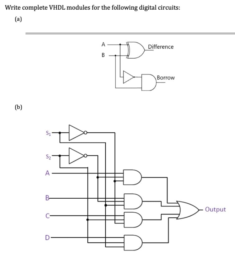
Write complete VHDL modules for the following digital circuits: (a) A Difference Borrow (b) S1 S2 A B- Output D-


Q: 2) Write VHDL code of the circuit as shown in figure A AND2 INV XOR2 X2 OR3 AND2
A: library IEEE;use IEEE.STD_LOGIC_1164.ALL;use IEEE.STD_LOGIC_ARITH.ALL;use…
Q: A combinational logic circuit has an output F=a'b'c+a'c'd'+bc'd+acd. A static one hazard occurs when
A: Given logic function is, F= a'b'c+a'c'd'+bc'd+acd This function contains four variables a, b, c and…
Q: Given in the figure is PLA circuit, used to implement the Boolean functions f1(X1,X2,X3) and…
A: Solution Option C could be the answer F2=x1x2+x2'x3 Detailed explanation is given below
Q: Design an appropriate combinational circuit that implements a digital system with the following…
A: Design a combinational circuit which take 4bit input and it has 7 outputs to which connect with the…
Q: Given the expression below, build the equivalent digital circuit NAND implementation. X = AB+ CB +…
A:
Q: Design a logic circuit whose output is HIGH only when a majority of inputs A, B, and C are LOW. Draw…
A: Given Output is high when majority of inputs A,B,C are low. Consider A=0,B=0,C=0
Q: Implement the BCD-to-seven segment decoder circuit using NAND gates only. A CD a 1 1 1 1 1 1 1 1 1 1…
A: The solution to the given problem is below.
Q: Draw a circuit diagram of 4 bit full adder and full subtractor.
A: Screenshot of 4-bit Full Adder and full subtractor:
Q: Construct the circuit using RTL components for the function; F(A,B,C,D)=E(0,4,8,12,14).
A: RTL components refers to the Registers and combination circuits like MUX and adders. So let us…
Q: EXERCISES 1. Construct an A-O-l gate with CMOS basic logic gates. 2. Construct a "Product of Sum"…
A:
Q: pblem Expand the circuit in Figure 6-25 to a 16-bit comparator.
A: A 16 bit comparator
Q: Make a Seven-Segment electrical circuit on Proteus with outputs and inputs as follows:
A: Make a Seven-Segment electrical circuit on Proteus with outputs and inputs as follows:
Q: Determine the worst case delay of CMOS circuit with the expression F=((A.C)+B).(A’.C’) driving 8…
A: Given: Determine the worst case delay of CMOS circuit with the expression F=((A.C)+B).(A’.C’)…
Q: 4. Design a combinational circuit with four inputs, ABCD. If A+C=0, one indicator should be low. If…
A: We have to design a combinational circuit with four inputs A, B, C, D. When A+C =0 , 1st indicator…
Q: 1. Design a module with Verilog for a full substractor circuit,
A: Verilog Code for Full Subtractor using Half Subtractor
Q: H.W\| Design Half Adder logical circuit by using only NAND gate?
A: Half adder is a combinational circuit which performs simple addition of two bits. and it produces a…
Q: Design a 4-bit comparator using 2-input NAND gates only. Simplify the circuit as far as possible.…
A: Digital Comparator The Digital Comparator is another very useful combinational logic circuit used…
Q: ) Draw a D Flip-Flop circuit constructed in a Master/Slave configuration, using Transmission Gate…
A: Master-slave is a combination of two flip-flops connected in series, where one acts as a master and…
Q: Design a comparator to compare two eight bit numbers? Draw complete gate level diagram?
A: 8-Bit Comparator An 8-bit comparator compares the two 8-bit numbers by cascading of two 4-bit…
Q: A Output
A: Solution Output =A+B You can use single OR gate with inputs A, B Detailed explanation is given…
Q: 1. Draw the logic diagram of a two-to-four-line decoder using NAND gates only. Include an enable…
A: Decoder is a combinational circuit and the number of inputs are n then the number of outputs in the…
Q: Design a NAND Logic Circuit that is equivalent to the AOI circuit shown below: A B C D-z =BC +AC
A: Given logic circuit contains NOT, AND and OR gates. Given function is, Z=BC+AC
Q: Consider the multiplexer based logic circuit shown in the figure W MUX 1 MUX 1 S, Select one: O a.…
A: For a 2 × 1 MUX is shown above, the output function F is expressed as: F = S̅1 I0 + S1I1 i.e. when…
Q: 7- Assuming that a certain ASM chart has 3 states, the number mu using the multiplexer design…
A: ASM Charts: Algorithmic State Machine (ASM) Chart is a high-level flowchart-like notation to specify…
Q: The minimum number of 2 x 1 MUX required to implement a half-subtracter circuit when only basic…
A: Introduction :
Q: write VHDL code to implement a 4-bit adder of figure below. The circuit has two inputs (a, b) and…
A: Let’s see some points on VHDL.VHDL is a dataflow language.In this language every statement is…
Q: A parallel adder is a O a. A sequential and combinational circui O b. A combinational circuit
A: Option (b) is the correct option.
Q: Implement the digital circuit shown in figure below using VHDL. X 10 2:1 MUX → f y Q D Cik
A: A device, which is acting like a building block for digital circuits, called logical circuit. It…
Q: i) Propose a circuit which can sum together two 3-bit binary numbers. You can rely on notable…
A: We need to propose an adder circuit to add two 3-bit numbers.
Q: Implement the circuit defined by equation F(a,b,c,d) = E (0,5,6,7,11) using: 4-to-1 multiplexers and…
A: 4-to-1 multiplexers and logic gates
Q: Design a 4-bit weighted-resistor DAC whose full-scale output voltage is – 5 V. The logic levels are…
A: Question :-
Q: Determine the value of X and Y in the below given circuit implementation of function F(A, B, C) =…
A: Introduction
Q: Designs the following circuit using VHDL code > Half adder. > Z=A'.B + A.C. > Z=a. b. c + d + b'. >…
A: Design the following circuit using VHDL code Answer: Half adders are a basic building block for new…
Q: Plot the output waveform of the following circuit 16 -16
A:
Q: The circuit below has a 2-to-4 decoder with active high outputs connected to a 4-to-1 MUX. Derive an…
A: Decoder:A binary code of n bits is capable of representing up to 2^n distinct elements of coded…
Q: c) For binary to BCD conversion, we need a circuit to add 3 to a binary number when the number is…
A: Binary to BCD convertion: ; Inputs: TEMPH, TEMPL (16-bit binary number) ; Outputs: R0, R1, R2 (5…
Q: Implement the function F (A, B, C) = E (1, 2, 4, 5, 7) a. Using a 2x4 decoder and any logic gates.…
A: 1) Using a 2 x 4 decoder and any logic gates: F( A, B, C)= ∑( 1, 2, 4, 5, 7)
Q: 1. Implement the function below using only 2-input NAND gates. H(A, B, C, D, E) = ABCĒ + AB + AC +…
A: Implement the function below using only 2-input NAND gates. H(A, B, C, D, E) = ABCE + AB+ AC + AD +…
Q: HW: (a) Design a CMOS logic circuit that implements the logic function. f(A, B, C) = A + BC
A: Here is the solution:
Q: Using a 2x1 MUX and other gates and MSI components of your choice, design a device with the…
A: ans is given below
Q: multiplexer
A: We can implement 16x1 Multiplexer using 4x1 Multiplexers . We know that 4x1 Multiplexer has 4 data…
Q: Using VDHL, a logic circuit’s inputs and outputs are described in the(a) architecture (b)…
A: Using VDHL, a logic circuit’s inputs and outputs are described in the
Q: Build functionf (x1, X2, X3, X4) = II M(0, 2, 5, 6, 9, 14) using Shannon’s Expa and the given…
A:
Q: 2. Draw a complete logic diagram for the 4-bit parallel adder 3. From 2, test your logic diagram…
A: A full adder is a digital circuit that performs addition. A full adder adds three one-bit binary…
Q: Using NAND gates, one 3-8 decoder, and 1 2-1 MUX, design a combination circuit with two outputs…
A:
Q: mplement a full – adder circuit using 4 to 1 multiplexers. -
A:
Q: Draw the internal logic circuit for 3-8 decoder circuit with enable
A: Decoder is a combinational circuit which contains n inputs and 2n outputs. Given circuit is 3-8…

Step by step
Solved in 2 steps


- Draw the circuit and obtain the truth table of the VHDL module below module SAM(a, b, c, M, S);input a,b,c;output M;output S;wire d,e,f;xor(S,a,b,c);and(d,~a,b);and(e,b,c);and(f,~a,c);or(M,d,e,f);endmoduleDesign an appropriate combinational circuit that implements a digital system with the following output functions an AC remote: ON, OFF, MODE, SHIFT, FAN, SMART, SWING, ECO using a decoder.draw a QPSK demodulator circuit using different circuit components. stop rejecting questions
- Write a signal assignment statement for use in the architecture of notif0_vhdl, a three-state inverter component having output signal y_out, input signal x_in, and active-low control signal enable_b.the following combinational circuit takes two 4-bit numbers( A , B) and takes a single bit control input5. Design an appropriate combinational circuit that implements a digital system with the following output functions: ROR, SHL, AND, XOR, ADD, DIV, SUB, MOV using a decoder. 6. Design the circuit diagram and truth table for the Boolean expression : F = (A’B) + (C’B).
- B) redraw the circuit from (a) using only NAND gates.Design a combinational logic circuit that takes a 3–bit input and has one output P. The P output should be active high only when the inputs corresponds to a prime number Note: the prime numbers: Prime numbers are 2, 3, 5, 7… Select one: a. P= AC+B b. P= A'C+A'B c. P= AC+A'B d. P= AC+A'B'Find the maxterm expansion and Develop a maxterm digital circuit based off the truth table