3. A “J309" JFET transistor is to be used as a small signal amplifier as shown below. The circuit is to have Av and a maximum Ips = 8mA with VDD = 20V. Obtain a manufacturer's datasheet for this transistor. From the datasheet, determine maximum values for VDs and Vas, Vas-off (range), Ipss (range), and the minimum a. for the common-source forward transconductance, gfs, (@1kHz). b. Write out the equation for Ay (as a function of Rp, Rs, and grs). C. Write out the equation for Ips (in terms of VpD, RD, and Rs).
3. A “J309" JFET transistor is to be used as a small signal amplifier as shown below. The circuit is to have Av and a maximum Ips = 8mA with VDD = 20V. Obtain a manufacturer's datasheet for this transistor. From the datasheet, determine maximum values for VDs and Vas, Vas-off (range), Ipss (range), and the minimum a. for the common-source forward transconductance, gfs, (@1kHz). b. Write out the equation for Ay (as a function of Rp, Rs, and grs). C. Write out the equation for Ips (in terms of VpD, RD, and Rs).

Introductory Circuit Analysis (13th Edition)
13th Edition
ISBN:9780133923605
Author:Robert L. Boylestad
Publisher:Robert L. Boylestad
Chapter1: Introduction
Section: Chapter Questions
Problem 1P: Visit your local library (at school or home) and describe the extent to which it provides literature...

Related questions

Question
100%
data sheets are included
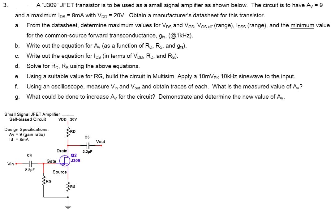
Transcribed Image Text:3.
A “J309" JFET transistor is to be used as a small signal amplifier as shown below. The circuit is to have Ay = 9
and a maximum Ips = 8mA with VDp = 20V. Obtain a manufacturer's datasheet for this transistor.
From the datasheet, determine maximum values for Vps and VGs, VGs-off (range), Ipss (range), and the minimum value
a.
for the common-source forward transconductance, grs, (@1kHz).
b.
Write out the equation for Av (as a function of Rp, Rs, and grs).
C.
Write out the equation for Ips (in terms of VDD, Rp, and Rs).
d.
Solve for RD, Rs using the above equations.
е.
Using a suitable value for RG, build the circuit in Multisim. Apply a 10mVPK 1OkHz sinewave to the input.
f.
Using an oscilloscope, measure Vin and Vout and obtain traces of each. What is the measured value of Av?
g.
What could be done to increase Ay for the circuit? Demonstrate and determine the new value of Ay.
Small Signal JFET Amplifier
Self-biased Circuit
VDD 20V
Design Specifications:
Av = 9 (gain ratio)
Id = 8mA
RD
C5
Vout
Drain
Q2
2.2µF
C4
Gate
J309
Vin
2.2µF
Source
RG
RS
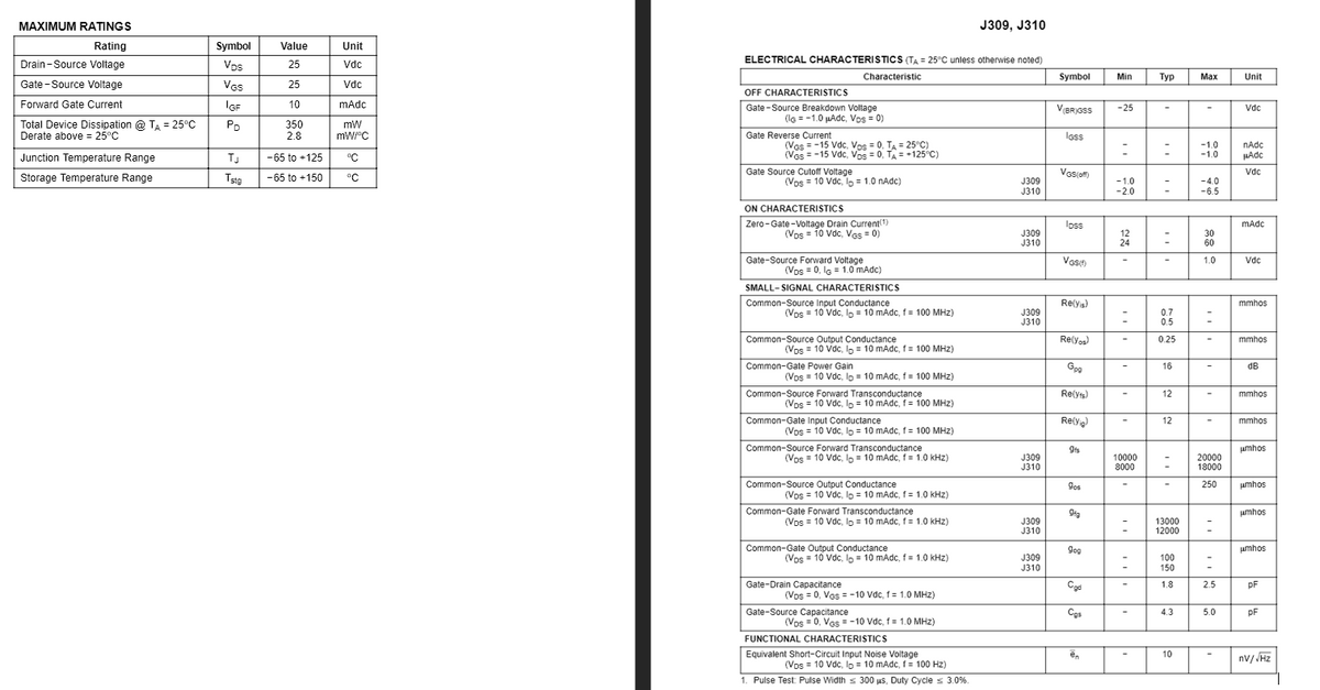
Transcribed Image Text:MAXIMUM RATINGS
J309, J310
Rating
Symbol
Value
Unit
ELECTRICAL CHARACTERIS TICS (TA = 25°C unless otherwise noted)
Drain -Source Voltage
Vps
25
Vdc
Characteristic
Symbol
Min
Тур
Маx
Unit
Gate -Source Voltage
Ves
25
Vdc
OFF CHARACTERISTICS
Forward Gate Current
IGF
10
mAdc
Gate -Source Breakdown Voltage
(lG = -1.0 µAdc, Vos = 0)
VBRYGSS
-25
Vdc
-
Total Device Dissipation @ TA = 25°C
Derate above = 25°C
350
2.8
mW
Gate Reverse Current
Isss
(Ves = -15 Vdc, Vos = 0, TA = 25°C)
(Vos = -15 Vdc, Vos = 0, TA = +125°C)
-1.0
-1.0
nAdc
HAdc
Junction Temperature Range
TJ
-65 to +125
°C
Storage Temperature Range
Tstg
Gate Source Cutoff Voltage
Vosiom
Vdc
-65 to +150
°C
(Vos = 10 Vdc, lo = 1.0 nAdc)
J309
J310
-1.0
-2.0
-4.0
-6.5
ON CHARACTERISTICS
Zero-Gate -Voltage Drain Current(1)
(Vos = 10 Vdc, Ves = 0)
Ioss
mAdc
J309
J310
12
24
30
60
Gate-Source Forward Voltage
(Vos = 0, le = 1.0 mAdc)
Vesin
1.0
Vdc
SMALL- SIGNAL CHARACTERISTICS
Common-Source Input Conductance
Re(ys)
mmhos
(Vos = 10 Vdc, lo = 10 mAdc, f= 100 MHz)
J309
J310
0.7
0.5
Common-Source Output Conductance
Re(yos)
0.25
mmhos
(Vos = 10 Vdc, lo = 10 mAdc, f= 100 MHz)
Common-Gate Power Gain
Gog
16
dB
-
(Vos = 10 Vdc, lo = 10 mAdc, f = 100 MHz)
Common-Source Forward Transconductance
Re(yts)
12
mmhos
(Vos = 10 Vdc, lo = 10 mAdc, f= 100 MHz
Common-Gate Input Conductance
Re(yig)
12
mmhos
(Vos = 10 Vdc, Io = 10 mAdc, 1 = 100 MHz)
Common-Source Forward Transconductance
9is
umhos
(Vos = 10 Vdc, lo = 10 mAdc, f = 1.0 kHz)
J309
J310
10000
8000
20000
18000
Common-Source Output Conductance
Gos
250
umhos
(Vos = 10 Vdc, Io = 10 mAdc, f= 1.0 kHz)
Common-Gate Forward Transconductance
umhos
(Vos = 10 Vdc, lp = 10 mAdc, f = 1.0 kHz)
J309
J310
13000
12000
Common-Gate Output Conductance
Gog
umhos
(Vos = 10 Vdc, lo = 10 mAdc, f = 1.0 kHz)
J309
J310
100
150
Gate-Drain Capacitance
Cad
1.8
2.5
pF
(Vos = 0, Vos = -10 Vdc, 1= 1.0 MHz)
Gate-Source Capacitance
Ces
4.3
5.0
pF
(Vos = 0, VGs = -10 Vdc, f= 1.0 MHz)
FUNCTIONAL CHARACTERISTICS
Equivalent Short-Circuit Input Noise Voltage
en
10
nV/ /Hz
-
(Vos = 10 Vdc, lo = 10 mAdc, f = 100 Hz)
1. Pulse Test: Pulse Width s 300 us, Duty Cycle s 3.0%.
Expert Solution
This question has been solved!
Explore an expertly crafted, step-by-step solution for a thorough understanding of key concepts.

Step by step
Solved in 2 steps

Knowledge Booster


Learn more about
Need a deep-dive on the concept behind this application? Look no further. Learn more about this topic, electrical-engineering and related others by exploring similar questions and additional content below.Recommended textbooks for you
Introductory Circuit Analysis (13th Edition)
Electrical Engineering
ISBN:
9780133923605
Author:
Robert L. Boylestad
Publisher:
PEARSON

Delmar's Standard Textbook Of Electricity
Electrical Engineering
ISBN:
9781337900348
Author:
Stephen L. Herman
Publisher:
Cengage Learning

Programmable Logic Controllers
Electrical Engineering
ISBN:
9780073373843
Author:
Frank D. Petruzella
Publisher:
McGraw-Hill Education
Introductory Circuit Analysis (13th Edition)
Electrical Engineering
ISBN:
9780133923605
Author:
Robert L. Boylestad
Publisher:
PEARSON
Delmar's Standard Textbook Of Electricity
Electrical Engineering
ISBN:
9781337900348
Author:
Stephen L. Herman
Publisher:
Cengage Learning
Programmable Logic Controllers
Electrical Engineering
ISBN:
9780073373843
Author:
Frank D. Petruzella
Publisher:
McGraw-Hill Education

Fundamentals of Electric Circuits
Electrical Engineering
ISBN:
9780078028229
Author:
Charles K Alexander, Matthew Sadiku
Publisher:
McGraw-Hill Education

Electric Circuits. (11th Edition)
Electrical Engineering
ISBN:
9780134746968
Author:
James W. Nilsson, Susan Riedel
Publisher:
PEARSON

Engineering Electromagnetics
Electrical Engineering
ISBN:
9780078028151
Author:
Hayt, William H. (william Hart), Jr, BUCK, John A.
Publisher:
Mcgraw-hill Education,