5) Realize the following functions using decoder and logic gates. a. Implement f(w1,w2,w3) = m (0,1,2,3,4,5,7) using 3-8 decoder and OR gate. b. Implement f(w1,w2,w3) = Em (0,4,5,6) using 3-8 decoder and AND gate. c. Implement f(w,x.y,z) = Em (0,4,7,12,14) using 3-8 decoder and logic gate.
5) Realize the following functions using decoder and logic gates. a. Implement f(w1,w2,w3) = m (0,1,2,3,4,5,7) using 3-8 decoder and OR gate. b. Implement f(w1,w2,w3) = Em (0,4,5,6) using 3-8 decoder and AND gate. c. Implement f(w,x.y,z) = Em (0,4,7,12,14) using 3-8 decoder and logic gate.

Chapter22: Sequence Control
Section: Chapter Questions
Problem 6SQ: Draw a symbol for a solid-state logic element AND.

Related questions
Question
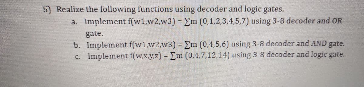
Transcribed Image Text:5) Realize the following functions using decoder and logic gates.
a. Implement f(w1,w2,w3) = Em (0,1,2,3,4,5,7) using 3-8 decoder and OR
gate.
b. Implement f(w1,w2,w3) = Em (0,4,5,6) using 3-8 decoder and AND gate.
c. Implement f(w,x,y,z) = Em (0,4,7,12,14) using 3-8 decoder and logic gate.
Expert Solution
This question has been solved!
Explore an expertly crafted, step-by-step solution for a thorough understanding of key concepts.

This is a popular solution!

Trending now
This is a popular solution!

Step by step
Solved in 4 steps with 8 images

Knowledge Booster


Learn more about
Need a deep-dive on the concept behind this application? Look no further. Learn more about this topic, electrical-engineering and related others by exploring similar questions and additional content below.Recommended textbooks for you