A cascaded amplifiers and their respective gains and noise figures are shown in Figure Q2(c). Compare the overall noise figure in this current arrangement and with the new arrangement when Amplifier B and C are interchanged. A B
A cascaded amplifiers and their respective gains and noise figures are shown in Figure Q2(c). Compare the overall noise figure in this current arrangement and with the new arrangement when Amplifier B and C are interchanged. A B

Power System Analysis and Design (MindTap Course List)
6th Edition
ISBN:9781305632134
Author:J. Duncan Glover, Thomas Overbye, Mulukutla S. Sarma
Publisher:J. Duncan Glover, Thomas Overbye, Mulukutla S. Sarma
Chapter12: Power System Controls
Section: Chapter Questions
Problem 12.3P

Related questions
Question
100%
Answer it
I will upvote
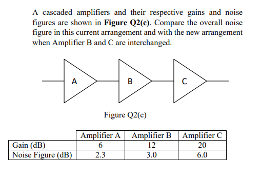
Transcribed Image Text:A cascaded amplifiers and their respective gains and noise
figures are shown in Figure Q2(c). Compare the overall noise
figure in this current arrangement and with the new arrangement
when Amplifier B and C are interchanged.
A
B
C
Figure Q2(c)
Amplifier A Amplifier B
Amplifier C
Gain (dB)
Noise Figure (dB)
6
12
20
2.3
3.0
6.0
Expert Solution
This question has been solved!
Explore an expertly crafted, step-by-step solution for a thorough understanding of key concepts.

This is a popular solution!

Trending now
This is a popular solution!

Step by step
Solved in 2 steps with 2 images

Knowledge Booster


Learn more about
Need a deep-dive on the concept behind this application? Look no further. Learn more about this topic, electrical-engineering and related others by exploring similar questions and additional content below.Recommended textbooks for you
Power System Analysis and Design (MindTap Course …
Electrical Engineering
ISBN:
9781305632134
Author:
J. Duncan Glover, Thomas Overbye, Mulukutla S. Sarma
Publisher:
Cengage Learning
Power System Analysis and Design (MindTap Course …
Electrical Engineering
ISBN:
9781305632134
Author:
J. Duncan Glover, Thomas Overbye, Mulukutla S. Sarma
Publisher:
Cengage Learning