a) Design (Find the values of W/L for NMOS and PMOS) a reference CMOS inverter to achieve a delay of 250ps when driving a 0.2pF load using 3.3V power supply. Assume K'n= 100 µA/V², K'p= 40 µA/V², VTN=-VTP= 0.75 V. Find the rise and fall times, Tp, TPHL and TPLH for the logic gate and compar them with results from simulation and plot transient response. b) Verify your design in part(a) using PSPICE or Multisim package. PULSE SOURCE DESCRIPTION (VS) Mp Initial voltage Peak voltage Delay time Rise time Vo VDD 3.3 V 3.3 V lie MN c0.2 pF 50 ps 50 ps V, Fall time Pulse width 2.95 ns Pulse period 6 ns ts tr TPLH, TPHL, TP Calculated Simulated % Difference
a) Design (Find the values of W/L for NMOS and PMOS) a reference CMOS inverter to achieve a delay of 250ps when driving a 0.2pF load using 3.3V power supply. Assume K'n= 100 µA/V², K'p= 40 µA/V², VTN=-VTP= 0.75 V. Find the rise and fall times, Tp, TPHL and TPLH for the logic gate and compar them with results from simulation and plot transient response. b) Verify your design in part(a) using PSPICE or Multisim package. PULSE SOURCE DESCRIPTION (VS) Mp Initial voltage Peak voltage Delay time Rise time Vo VDD 3.3 V 3.3 V lie MN c0.2 pF 50 ps 50 ps V, Fall time Pulse width 2.95 ns Pulse period 6 ns ts tr TPLH, TPHL, TP Calculated Simulated % Difference

Introductory Circuit Analysis (13th Edition)
13th Edition
ISBN:9780133923605
Author:Robert L. Boylestad
Publisher:Robert L. Boylestad
Chapter1: Introduction
Section: Chapter Questions
Problem 1P: Visit your local library (at school or home) and describe the extent to which it provides literature...

Related questions
Question
100%
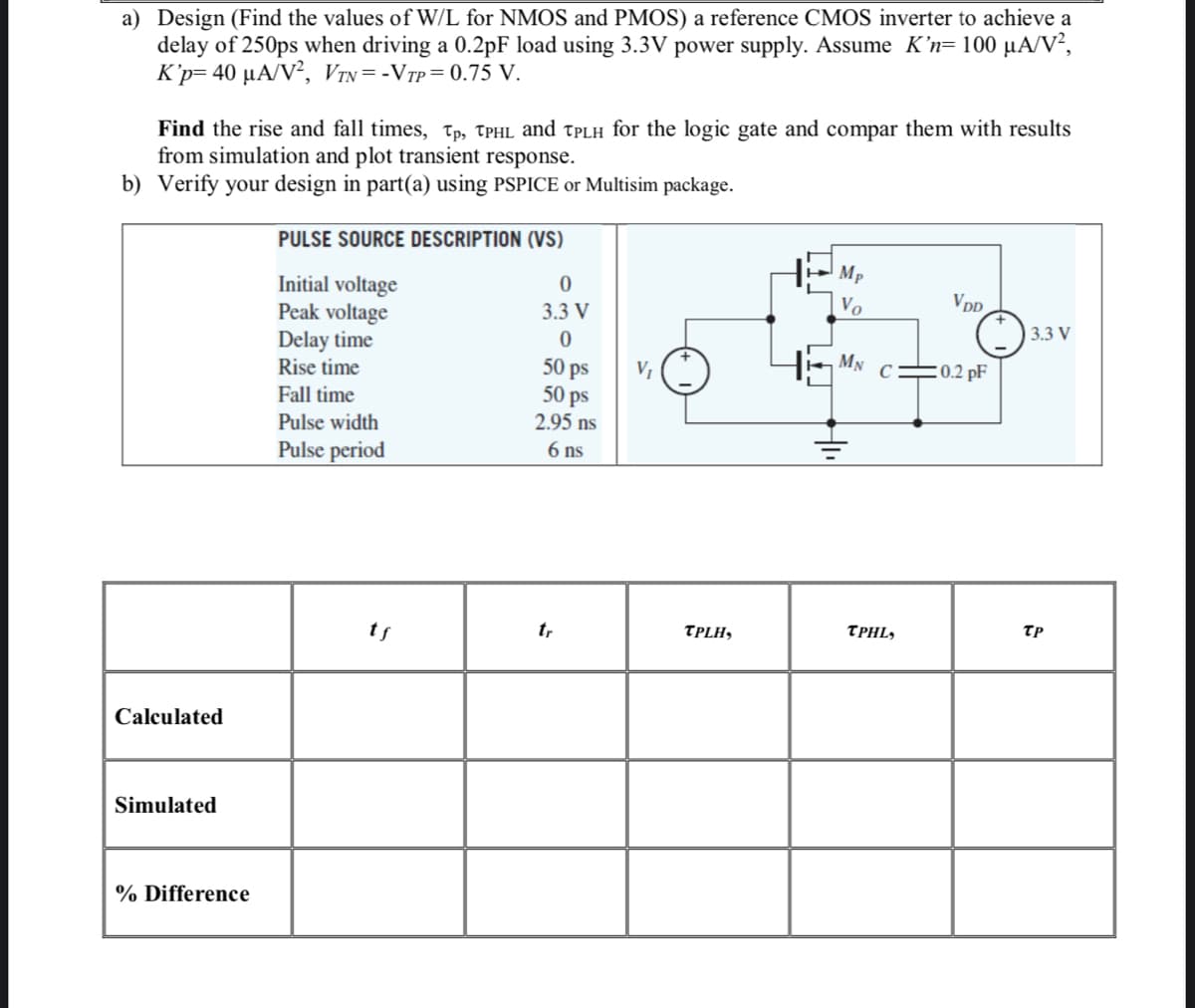
Transcribed Image Text:a) Design (Find the values of W/L for NMOS and PMOS) a reference CMOS inverter to achieve a
delay of 250ps when driving a 0.2pF load using 3.3V power supply. Assume K'n= 100 µA/V²,
K'p= 40 µA/V², VrN=-VTp=0.75 V.
Find the rise and fall times, Tp, TPHL and TPLH for the logic gate and compar them with results
from simulation and plot transient response.
b) Verify your design in part(a) using PSPICE or Multisim package.
PULSE SOURCE DESCRIPTION (VS)
Mp
Initial voltage
Peak voltage
Delay time
Rise time
Vo
VDD
3.3 V
3.3 V
MN
C=0.2 pF
50 ps
50 ps
2.95 ns
V,
Fall time
Pulse width
Pulse period
6 ns
tf
t,
TPLH,
TPHL,
TP
Calculated
Simulated
% Difference
Expert Solution
This question has been solved!
Explore an expertly crafted, step-by-step solution for a thorough understanding of key concepts.

Step by step
Solved in 4 steps with 4 images

Knowledge Booster


Learn more about
Need a deep-dive on the concept behind this application? Look no further. Learn more about this topic, electrical-engineering and related others by exploring similar questions and additional content below.Recommended textbooks for you
Introductory Circuit Analysis (13th Edition)
Electrical Engineering
ISBN:
9780133923605
Author:
Robert L. Boylestad
Publisher:
PEARSON

Delmar's Standard Textbook Of Electricity
Electrical Engineering
ISBN:
9781337900348
Author:
Stephen L. Herman
Publisher:
Cengage Learning

Programmable Logic Controllers
Electrical Engineering
ISBN:
9780073373843
Author:
Frank D. Petruzella
Publisher:
McGraw-Hill Education
Introductory Circuit Analysis (13th Edition)
Electrical Engineering
ISBN:
9780133923605
Author:
Robert L. Boylestad
Publisher:
PEARSON
Delmar's Standard Textbook Of Electricity
Electrical Engineering
ISBN:
9781337900348
Author:
Stephen L. Herman
Publisher:
Cengage Learning
Programmable Logic Controllers
Electrical Engineering
ISBN:
9780073373843
Author:
Frank D. Petruzella
Publisher:
McGraw-Hill Education

Fundamentals of Electric Circuits
Electrical Engineering
ISBN:
9780078028229
Author:
Charles K Alexander, Matthew Sadiku
Publisher:
McGraw-Hill Education

Electric Circuits. (11th Edition)
Electrical Engineering
ISBN:
9780134746968
Author:
James W. Nilsson, Susan Riedel
Publisher:
PEARSON

Engineering Electromagnetics
Electrical Engineering
ISBN:
9780078028151
Author:
Hayt, William H. (william Hart), Jr, BUCK, John A.
Publisher:
Mcgraw-hill Education,