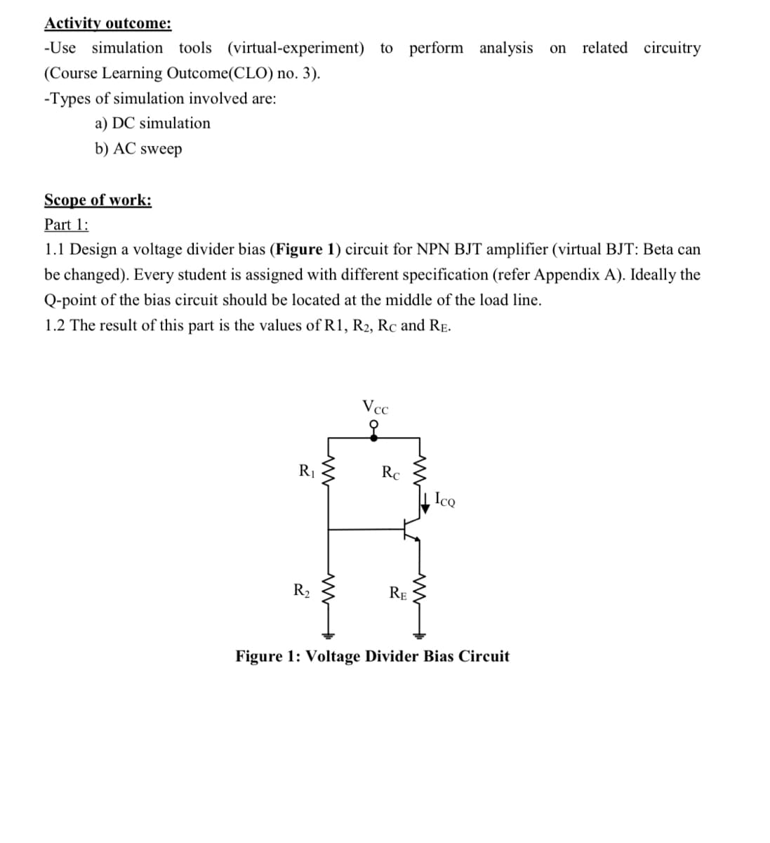
Activity outcome: -Use simulation tools (virtual-experiment) to perform analysis on related circuitry (Course Learning Outcome(CLO) no. 3). -Types of simulation involved are: a) DC simulation b) AC sweep Scope of work: Part 1: 1.1 Design a voltage divider bias (Figure 1) circuit for NPN BJT amplifier (virtual BJT: Beta can be changed). Every student is assigned with different specification (refer Appendix A). Ideally the Q-point of the bias circuit should be located at the middle of the load line. 1.2 The result of this part is the values of R1, R2, Rc and RE. Vcc to R1 Rc IcQ R2 RE Figure 1: Voltage Divider Bias Circuit
Activity outcome: -Use simulation tools (virtual-experiment) to perform analysis on related circuitry (Course Learning Outcome(CLO) no. 3). -Types of simulation involved are: a) DC simulation b) AC sweep Scope of work: Part 1: 1.1 Design a voltage divider bias (Figure 1) circuit for NPN BJT amplifier (virtual BJT: Beta can be changed). Every student is assigned with different specification (refer Appendix A). Ideally the Q-point of the bias circuit should be located at the middle of the load line. 1.2 The result of this part is the values of R1, R2, Rc and RE. Vcc to R1 Rc IcQ R2 RE Figure 1: Voltage Divider Bias Circuit

Chapter25: Television, Telephone, And Low-voltage Signal Systems
Section25.1: Television Circuit
Problem 5R: From a cost standpoint, which system is more economical to install: a master amplifier distribution...

Related questions
Question
VCC(V):15
ICsat(mA):8
Beta:150
Transcribed Image Text:Activity outcome:
-Use simulation tools (virtual-experiment) to perform analysis on
related circuitry
(Course Learning Outcome(CLO) no. 3).
-Types of simulation involved are:
a) DC simulation
b) AC sweep
Scope of work:
Part 1:
1.1 Design a voltage divider bias (Figure 1) circuit for NPN BJT amplifier (virtual BJT: Beta can
be changed). Every student is assigned with different specification (refer Appendix A). Ideally the
Q-point of the bias circuit should be located at the middle of the load line.
1.2 The result of this part
the values of R1, R2, Rc and RE.
Vcc
R1
Rc
IcQ
R2
RE
Figure 1: Voltage Divider Bias Circuit
Transcribed Image Text:Part 2:
2.1 Based on the calculation in Part 1, choose the practical/standard resistor value by referring to
Appendix B.
2.2 By using the standard resistor values, construct the circuit in Figure 1 and simulate (DC
simulation) to obtain the Icq and VCEQ.
2.3 For the simulation, you need to add current meter (series connection at collector terminal) and
voltage meter (parallel connection between collector and emitter).
2.4 Discuss the result by commenting whether the obtained Q-point is suitable for the amplifier
application.
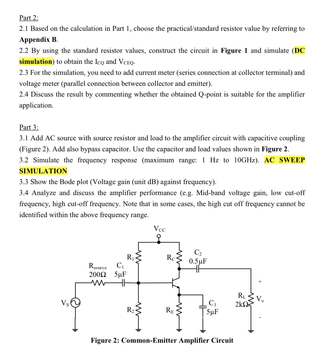
Part 3:
3.1 Add AC source with source resistor and loa
to the amplifier circuit with capacitive coupling
(Figure 2). Add also bypass capacitor. Use the capacitor and load values shown in Figure 2.
3.2 Simulate the frequency response (maximum range: 1 Hz to 10GHZ). AC SWEEP
SIMULATION
3.3 Show the Bode plot (Voltage gain (unit dB) against frequency).
3.4 Analyze and discuss the amplifier performance (e.g. Mid-band voltage gain, low cut-off
frequency, high cut-off frequency. Note that in some cases, the high cut off frequency cannot be
identified within the above frequency range.
Vcc
C2
0.5µF
R1
С
2002 5µF
Rc
source
+
RL
2kΩ
Vs
C3
R2
RE
SµF
Figure 2: Common-Emitter Amplifier Circuit
Expert Solution
This question has been solved!
Explore an expertly crafted, step-by-step solution for a thorough understanding of key concepts.

Step by step
Solved in 2 steps with 2 images

Knowledge Booster


Learn more about
Need a deep-dive on the concept behind this application? Look no further. Learn more about this topic, electrical-engineering and related others by exploring similar questions and additional content below.Recommended textbooks for you
EBK ELECTRICAL WIRING RESIDENTIAL
Electrical Engineering
ISBN:
9781337516549
Author:
Simmons
Publisher:
CENGAGE LEARNING - CONSIGNMENT
EBK ELECTRICAL WIRING RESIDENTIAL
Electrical Engineering
ISBN:
9781337516549
Author:
Simmons
Publisher:
CENGAGE LEARNING - CONSIGNMENT