Calculate (Ar). (Z), and (Zof) for the amplifier of Figure. Assume (he = 50), (he=1 kn), (h, = ho - 0), and identical transistors I+24 V 5.6 kn 120 kn VHHO Zof 5.6 kn 47 kn 33 kn Zir 4.1 kn 4.7 k2: 0.2 kn H
Calculate (Ar). (Z), and (Zof) for the amplifier of Figure. Assume (he = 50), (he=1 kn), (h, = ho - 0), and identical transistors I+24 V 5.6 kn 120 kn VHHO Zof 5.6 kn 47 kn 33 kn Zir 4.1 kn 4.7 k2: 0.2 kn H

Chapter25: Television, Telephone, And Low-voltage Signal Systems
Section25.1: Television Circuit
Problem 5R: From a cost standpoint, which system is more economical to install: a master amplifier distribution...

Related questions

Question
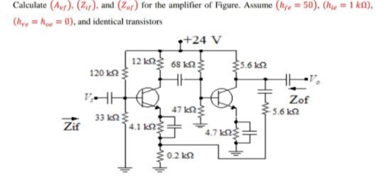
Transcribed Image Text:Calculate (Ar). (Z), and (Zof) for the amplifier of Figure. Assume (he = 50), (he=1 kn),
(h, = ho - 0), and identical transistors
I+24 V
5.6 kn
120 kn
VHHO
Zof
5.6 kn
47 kn
33 kn
Zir
4.1 kn
4.7 k2:
0.2 kn
H
Expert Solution
This question has been solved!
Explore an expertly crafted, step-by-step solution for a thorough understanding of key concepts.

Step by step
Solved in 3 steps with 3 images

Knowledge Booster


Learn more about
Need a deep-dive on the concept behind this application? Look no further. Learn more about this topic, electrical-engineering and related others by exploring similar questions and additional content below.Recommended textbooks for you
EBK ELECTRICAL WIRING RESIDENTIAL
Electrical Engineering
ISBN:
9781337516549
Author:
Simmons
Publisher:
CENGAGE LEARNING - CONSIGNMENT
EBK ELECTRICAL WIRING RESIDENTIAL
Electrical Engineering
ISBN:
9781337516549
Author:
Simmons
Publisher:
CENGAGE LEARNING - CONSIGNMENT