Calculate current gain, input and output impedance, and linearity. Beta = 90 IS = 2E-15
Calculate current gain, input and output impedance, and linearity. Beta = 90 IS = 2E-15

Delmar's Standard Textbook Of Electricity
7th Edition
ISBN:9781337900348
Author:Stephen L. Herman
Publisher:Stephen L. Herman
Chapter30: Dc Motors
Section: Chapter Questions
Problem 6RQ: What is CEMF?

Related questions
Question
Calculate current gain, input and output impedance, and linearity.
Beta = 90
IS = 2E-15
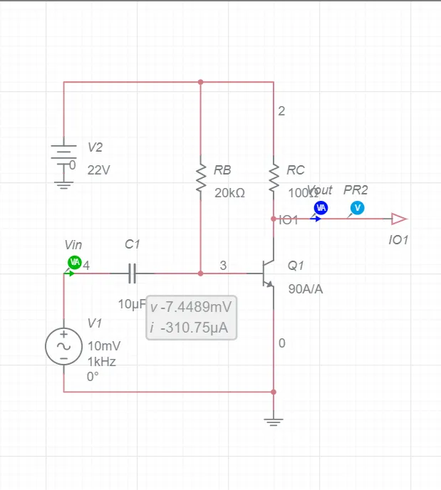
Transcribed Image Text:2
V2
22V
RB
RC
20KQ
100kput PR2
Vin
C1
101
VA
3
Q1
H
90A/A
10µF v -7.4489mV
i-310.75µA
V1
10mV
1kHz
0°
Expert Solution
This question has been solved!
Explore an expertly crafted, step-by-step solution for a thorough understanding of key concepts.

Step by step
Solved in 5 steps with 3 images

Recommended textbooks for you
Delmar's Standard Textbook Of Electricity
Electrical Engineering
ISBN:
9781337900348
Author:
Stephen L. Herman
Publisher:
Cengage Learning

EBK ELECTRICAL WIRING RESIDENTIAL
Electrical Engineering
ISBN:
9781337516549
Author:
Simmons
Publisher:
CENGAGE LEARNING - CONSIGNMENT
Delmar's Standard Textbook Of Electricity
Electrical Engineering
ISBN:
9781337900348
Author:
Stephen L. Herman
Publisher:
Cengage Learning
EBK ELECTRICAL WIRING RESIDENTIAL
Electrical Engineering
ISBN:
9781337516549
Author:
Simmons
Publisher:
CENGAGE LEARNING - CONSIGNMENT