circuits, pleaseeeee solve questionnn B :5

Introductory Circuit Analysis (13th Edition)
13th Edition
ISBN:9780133923605
Author:Robert L. Boylestad
Publisher:Robert L. Boylestad
Chapter1: Introduction
Section: Chapter Questions
Problem 1P: Visit your local library (at school or home) and describe the extent to which it provides literature...

Related questions

Question
circuits, pleaseeeee solve questionnn B :5
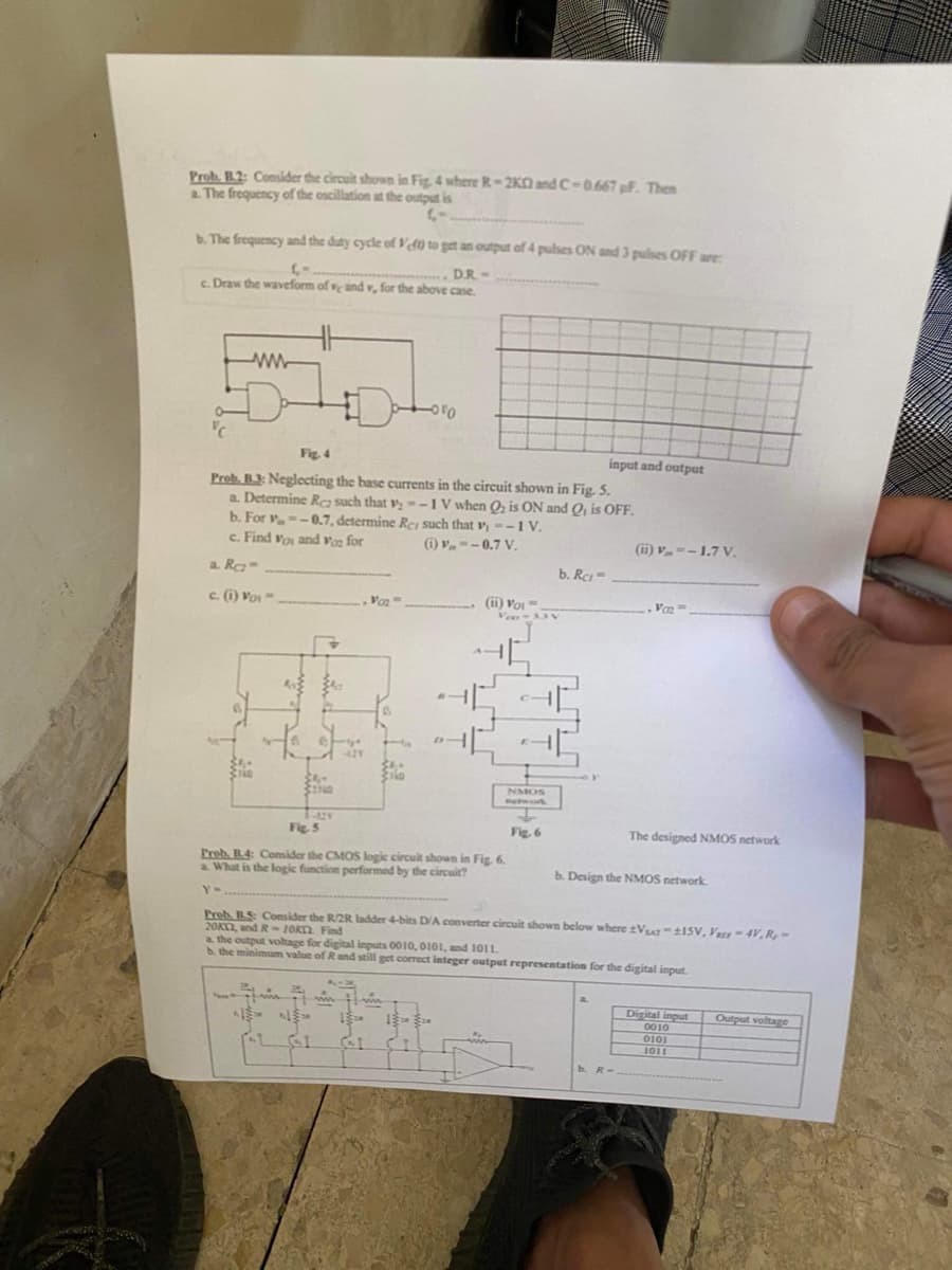
Transcribed Image Text:Prob. B.2: Consider the circuit shown in Fig. 4 where R-2K and C-0.667 pF. Then
a. The frequency of the oscillation at the output is
C-
b. The frequency and the duty cycle of Vf0 to get an output of 4 pulses ON and 3 pulses OFF are:
(-.
D.R. -
c. Draw the waveform of ve and v, for the above case.
wwwww
HH
Fig. 4
Prob. B3: Neglecting the base currents in the circuit shown in Fig. 5.
a. Determine Rez such that v₂-1 V when Q₂ is ON and Q₁ is OFF.
b. For v=-0.7, determine Re, such that v, --1 V.
c. Find Vos and Voz for
(1)--0.7 V.
a. Rez-
c. (1) VOI-
34.
777
421
AL GI
-010
Van'
wwwwww
(ii) Voi
41
041
Fig. 5
Preb. B.4: Consider the CMOS logic circuit shown in Fig. 6.
a. What is the logic function performed by the circuit?
Y-
Veo-33V
NMOS
Network
b. Rc-
Fig. 6
input and output
(ii) V-1.7 V.
Prob. B.S: Consider the R/2R ladder 4-bits D/A converter circuit shown below where Vsr-115V, V-4V, R,-
20KC2, and R-10KT2. Find
Vo₂=
a the output voltage for digital inputs 0010, 0101, and 1011.
b. the minimum value of R and still get correct integer output representation for the digital input.
The designed NMOS network
b. Design the NMOS network.
b. R-
Digital input
0010
0101
1011
Output voltage
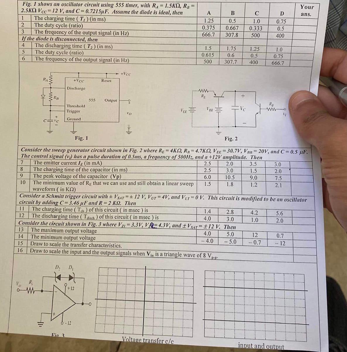
Transcribed Image Text:Fig. 1 shows an oscillator circuit using 555 timer, with RA = 1.5KQ, RB =
2.5KQ Vcc= 12 V, and C= 0.7215uF. Assume the diode is ideal, then
1
2
3
If the diode is disconnected, then
4
5
6
The charging time (T,) (in ms)
The duty cycle (ratio)
The frequency of the output signal (in Hz)
10
16
The discharging time (T₂) (in ms)
The duty cycle (ratio)
The frequency of the output signal (in Hz)
V R₁
RA
RB
11
+Vcc
Discharge
Threshold
Trigger
Ground
D,
Fig 3
Reset
555 Output
+12
5-12
+Vcc
45
vo
VEE
A
1.25
0.375
666.7
The minimum output voltage
Draw to scale the transfer characteristics.
Draw to scale the input and the output signals when Vin is a triangle wave of 8 Vp-p
1.5
0.615
500
Voltage transfer c/c
ww
RE
VER
Fig. 1
Fig. 2
Consider the sweep generator circuit shown in Fig. 2 where RE = 4KS2, RB = 4.7K2, VEE=30.7V, VBB= 20V, and C= 0.5 uF.
The control signal (v) has a pulse duration of 0.5ms, a frequency of 500Hz, and a +12V amplitude. Then
7
2.5
3.5
8
9
The emitter current I (in mA)
The charging time of the capacitor (in ms)
2.5
The peak voltage of the capacitor (Vp)
6.0
The minimum value of Rg that we can use and still obtain a linear sweep 1.5
waveform (in K2)
Consider a Schmitt trigger circuit with ± VSAT = 12 V, Vur=4V, and Vir=0 V. This circuit is modified to be an oscillator
circuit by adding C= 3.46 µF and R=2 KS2. Then
11 The charging time (Tch) of this circuit (in msec) is
2.8
12 The discharging time (Tdisch) of this circuit ( in msec ) is
3.0
Consider the circuit shown in Fig. 3 where Vzi = 3.3V, VA= 4.3V, and ± VSAT = ±12 V. Then
13 The maximum output voltage
4.0
5.0
14
-4.0
- 5.0
15
B
C
0.5
1.0
0.667 0.333
307.8
500
1.4
4.0
1.75
0.6
307.7
1.25
0.5
400
2.0
3.0
10.5
1.8
282
1.5
9.0
1.2
4.2
1.0
D
0.75
0.5
400
1.0
0.75
666.7
R₂
12
-0.7
LI
3.0
2.0
7.5
2.1
199
5.6
2.0
Your
ans.
0.7
- 12
input and output
Expert Solution
This question has been solved!
Explore an expertly crafted, step-by-step solution for a thorough understanding of key concepts.

Step by step
Solved in 2 steps

Knowledge Booster


Learn more about
Need a deep-dive on the concept behind this application? Look no further. Learn more about this topic, electrical-engineering and related others by exploring similar questions and additional content below.Recommended textbooks for you
Introductory Circuit Analysis (13th Edition)
Electrical Engineering
ISBN:
9780133923605
Author:
Robert L. Boylestad
Publisher:
PEARSON

Delmar's Standard Textbook Of Electricity
Electrical Engineering
ISBN:
9781337900348
Author:
Stephen L. Herman
Publisher:
Cengage Learning

Programmable Logic Controllers
Electrical Engineering
ISBN:
9780073373843
Author:
Frank D. Petruzella
Publisher:
McGraw-Hill Education
Introductory Circuit Analysis (13th Edition)
Electrical Engineering
ISBN:
9780133923605
Author:
Robert L. Boylestad
Publisher:
PEARSON
Delmar's Standard Textbook Of Electricity
Electrical Engineering
ISBN:
9781337900348
Author:
Stephen L. Herman
Publisher:
Cengage Learning
Programmable Logic Controllers
Electrical Engineering
ISBN:
9780073373843
Author:
Frank D. Petruzella
Publisher:
McGraw-Hill Education

Fundamentals of Electric Circuits
Electrical Engineering
ISBN:
9780078028229
Author:
Charles K Alexander, Matthew Sadiku
Publisher:
McGraw-Hill Education

Electric Circuits. (11th Edition)
Electrical Engineering
ISBN:
9780134746968
Author:
James W. Nilsson, Susan Riedel
Publisher:
PEARSON

Engineering Electromagnetics
Electrical Engineering
ISBN:
9780078028151
Author:
Hayt, William H. (william Hart), Jr, BUCK, John A.
Publisher:
Mcgraw-hill Education,