Construct the truth table of two input Ex-OR gate.


Q: Define full adder, make its truth table, solve for the equation of SUM and CARRY and draw its logic…
A: In Question: Define full adder, make its truth table, solve for the equation of SUM and CARRY and…
Q: Derive the truth table and draw the logic diagram of a full adder.
A:
Q: How many full adder circuits are needed to add 2 six- bit binary numbers? None of the given choices…
A:
Q: (а) АВ + АB + АBС (b) АВ(С + D) (с) (А + В)(В + А)
A:
Q: Design 2 bit binary comparator with its truth table and K-Map. With Explanation?
A: Comparator is a combinational circuit which is used for doing the comparison of bits. As the output…
Q: Q2. Reduce the following Boolean expression using Boolean identities then implement by using…
A: In this question we need to simplify the given Boolean expression. And implement it using NAND gate
Q: The boolean expression of an EX-OR gate is
A: Any digital system has logic gates . In other words logic gates form the building blocks of a…
Q: Draw a circuit and create a truth table for all combinations of a 3-input OR gate.
A: Let the inputs are A, B, and C, and the output is F. The boolean expression for the 3-input OR gate…
Q: Design a circuit for 3-bit binary addition using logic gates and write the truth table and…
A: 3 bit binary adition can be performed by using the full adder circuit. let the three bits are A , B…
Q: Given the expression below, implement the equivalent circuit. X- ABC + ABC + AB Y - ABC + AB + BC
A: Since you have posted multiple different question. we will solve the first question for you. To get…
Q: Write the truth table and draw the structure of the following i) Nand gate , ii)Ex-or gate
A: NAND gate and Ex-OR gate are multi-input, one output logic gates. NAND gate is a cascade combination…
Q: Explain and Design 4 bit binary comparator with truth table and K-Map?
A: Steps to design combinational logic circuits : Identify the number of inputs and the number of…
Q: Explain differences between Boolean and Binary additions.
A: Introduction: Boolean addition is similar OR gate logic. For example in OR gate logic 1+0=1 and…
Q: With relevant logic diagram and truth table explain the working of a two input EX-OR gate
A: EX-OR gate: It stands for exclusive OR. It's symbol is ⊕. Two input EX-OR gate is
Q: Construct the truth table for 4 bit Excess 3 to Binary code code converter. Use K-map for…
A: Let's consider the 4 bit excess 3 inputs are ABCD and the binary output is WXYZ. The invalid…
Q: Create a TRUTH TABLE, and draw the equivalent LOGIC DIAGRAM and TIMING DIAGRAM of the following…
A:
Q: Convert each of the following 8-bit two’s complement binary values to decimal. I)101101112 ii)…
A: This question belongs to digital electronics. It is based on the conversion of 2's complement into…
Q: a. Implement two variable AND gate and OR gate using NAND gates. Draw figure of your implementation…
A: The logic diagram of AND gate and its truth table is given as
Q: Define and Draw the schematic symbol for Logic Ex-OR Gate and give the corresponding truth table.
A: EX-OR is an inequality detector circuit of both inputs that are not the same the output of the EX-OR…
Q: (le:7.9) Extend the OR gate to have three inputs, A, B and C. Determine the truth table for the…
A: Logic circuit Now the truth table will be ABCY00000011010101111001101111011111
Q: 04. For the combinational circuit shown below, list the truth table and find the equations of Fa F,…
A: The given circuit is
Q: Design a 4-to-1 multiplexer using a 2-to-4 decoder and only AND and OR gates? Briefly explain how…
A:
Q: What are the minimum required gates (example: how many of what kind: like 5 of 2 inputs OR gates,…
A: DECODER: A decoder is a combinational circuit that converts binary code into decimal output. A…
Q: 8- If we were to build a truth table for a 16-input AND gate, how many different combinations of…
A: We are authorized to answer one question at a time, since you have not mentioned which question you…
Q: Design a binary multiplier that multiplies two 8-bit binary number by following design rules that…
A: 8-bit Multiplier: Circuit Diagram:
Q: Write the truth table of the following logic gates using three inputs AND, OR, NAND, NOR,
A:
Q: lean equations for the 3-input NOR gate and the 3-input NAND
A:
Q: Assuming you were tasked to create a Gray Code to BCD converter, design a truth table to accommodate…
A: BCD range is 0 to 9 ( decimal ) For four bit gray code possible value is 24 Which is 16 value . We…
Q: How could you design a circuit for adding/subtracting two binary numbers each one consists of 8 bit…
A: in this we have to perform addition/subtraction of two 8 bit binary numbers, for this we will use a…
Q: Consider a 4-input AND gate. How many rows would its truth table have ?
A: for the n input the number of rows of the truth table is 2n
Q: B) Simplify the following Boolean expression to a minimum number of literals and Implement using…
A: Consider the given expression, It is known that the multiplication of a variable with its…
Q: binational circuit shown below, list th Vhere A. B, and C are the inputs where ld a binary numbers…
A: The full adder is a combinational circuit which has three input and two output sum and carry.
Q: Given a switching function f(A, B,C, D) = A'BD + AC'D. a) Find its minterm and maxterm expansions.…
A: Given data FA,B,C,D=A,BD+AC,D
Q: Q2. Reduce the following Boolean expression using Boolean identities then implement by using…
A: Given, Y=AB+A¯B+AB¯+AB¯ Following boolean identities are used to simplify the above expression. 1.…
Q: Determine the truth table for a NOR-logic based full adder circuit.
A: Steps to find the Truth table and Logic Diagram Decide the number of input Generated output will…
Q: If the bitstream 10110011 is passed through a even parity checker, then what will be the parity bit?
A: When a bitstream passes through an even parity checker, then the parity checker checks the number of…
Q: Draw the truth table for a six-bit binary to two's complement converter and K-Map.
A: Basic problem on digital electronics.
Q: Write the Boolean expression for the 4-input OR gate
A: Given; Or gate with 4 input Calculate: Boolean expression
Q: Question 7: full adder: Sketch a circuit that uses five full-adders to add together three 2-bit…
A:
Q: For the circuit above: what is the correct sequence for JA input for a standard binary sequence of…
A:
Q: Design a circuit with a truth table that converts a number between 0 to 7 in decimal to binary then…
A: Design a circuit with a truth table that converts a number between 0 to 7 in decimal to binary then…
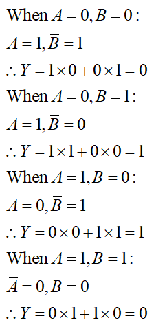
Construct the truth table of two input Ex-OR gate.
If A and B are the two inputs of a two input Ex-OR gate, then the output Y of the gate can be expressed as
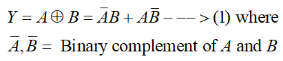
The truth table for the Ex-OR gate can be constructed in the following way:

Step by step
Solved in 3 steps with 3 images


- With relevant logic diagram and truth table explain the working of a two input EX-OR gateWhat are the 6 K-maps that come from this truth table of a 3-bit up/down binary counterDraw a truth table, Karnaugh diagram and logical gates circuit to show the functionof an even number detection circuit. That is, the output of the circuit will be one only ifthe value of the binary input is even. Assume three inputs.
- Fill in the truth table of the logic gateDraw the Truth Table of 4-bits Binary-to-Gray Code converter.Design A one bit, 3 input majority counter (voter) explain how it works in simple steps. include in the truth table of the circuit and also need to use the Boolean Algebra/Karnaugh Map to minimize the number of gates used in the design and build of such circuits.
- Construct the truth table for 4 bit Excess 3 to Binary code code converter. Use K-map for simplification and draw the circuit for 4 bit Excess 3 to Binary code Converter using AND, OR and Not gates in logisim Simulator.Explain and Design 4 bit binary comparator with truth table and K-Map?Draw the truth table for a six-bit binary to two's complement converter and K-Map.
- Design a circuit with a truth table that converts a number between 0 to 7 in decimal to binary then passes it to another component that outputs the number in the output line of the decimal number. Demonstrate the value of input and output using '7'. Discuss the process in your own words. [Hint: The number passes from encoder to decoder. Consider there is no enable pin in the decoder.]Use 2 of these decoders and any # of OR and NOT gates then implement a one-bit full binary adder. The standard inputs are a,b,cin and the outputs are s,cout. Please draw or display how the circuit should properly look.(1)Why the input lines of the MUX do not appear in the truth table with its logic values?