Design a decoder to convert the 421 BCD code to drive the 7-segment LED display to indicate alphabets A to H as shown in the following figure. This module must be built using minimum number of NOR gates ONLY. 1 2 3 5 88888888 A B C DE F G H Off = "0" On = '1' (i) Design the truth table for this module. (ii) Derive the logic equations for this module. (iii) Build this module using minimum number of NOR gates ONLY
Design a decoder to convert the 421 BCD code to drive the 7-segment LED display to indicate alphabets A to H as shown in the following figure. This module must be built using minimum number of NOR gates ONLY. 1 2 3 5 88888888 A B C DE F G H Off = "0" On = '1' (i) Design the truth table for this module. (ii) Derive the logic equations for this module. (iii) Build this module using minimum number of NOR gates ONLY

Chapter4: Processor Technology And Architecture
Section: Chapter Questions
Problem 14VE

Related questions
Question
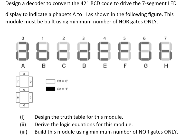
Transcribed Image Text:Design a decoder to convert the 421 BCD code to drive the 7-segment LED
display to indicate alphabets A to H as shown in the following figure. This
module must be built using minimum number of NOR gates ONLY.
2
3
5
6
7
88888888
A
B C D E F G H
b
Off = '0'
On = '1'
e
(i)
Design the truth table for this module.
(ii)
Derive the logic equations for this module.
(iii)
Build this module using minimum number of NOR gates ONLY.
Expert Solution
This question has been solved!
Explore an expertly crafted, step-by-step solution for a thorough understanding of key concepts.

Step by step
Solved in 2 steps with 2 images

Knowledge Booster


Learn more about
Need a deep-dive on the concept behind this application? Look no further. Learn more about this topic, computer-science and related others by exploring similar questions and additional content below.Recommended textbooks for you
Systems Architecture
Computer Science
ISBN:
9781305080195
Author:
Stephen D. Burd
Publisher:
Cengage Learning
Systems Architecture
Computer Science
ISBN:
9781305080195
Author:
Stephen D. Burd
Publisher:
Cengage Learning