Doe Do Dor Do Vị V3 Figure 2: Simulating delays with inverters. Let each inverter have delay A, then the delay between input u and outputs v1, V2, V3 are 2A, 4A, 6A, respectively. The logic value at the input u and any of the outputs v1, v2, V3 is the same. As part of the prelab work, lay out the circuit of Figure 2, separately from the lay out of the MUX circuit. Use a 74LS04 chip.
Doe Do Dor Do Vị V3 Figure 2: Simulating delays with inverters. Let each inverter have delay A, then the delay between input u and outputs v1, V2, V3 are 2A, 4A, 6A, respectively. The logic value at the input u and any of the outputs v1, v2, V3 is the same. As part of the prelab work, lay out the circuit of Figure 2, separately from the lay out of the MUX circuit. Use a 74LS04 chip.

Chapter22: Sequence Control
Section: Chapter Questions
Problem 6SQ: Draw a symbol for a solid-state logic element AND.

Related questions
Question
Transcribed Image Text:2
Transient Logic Values
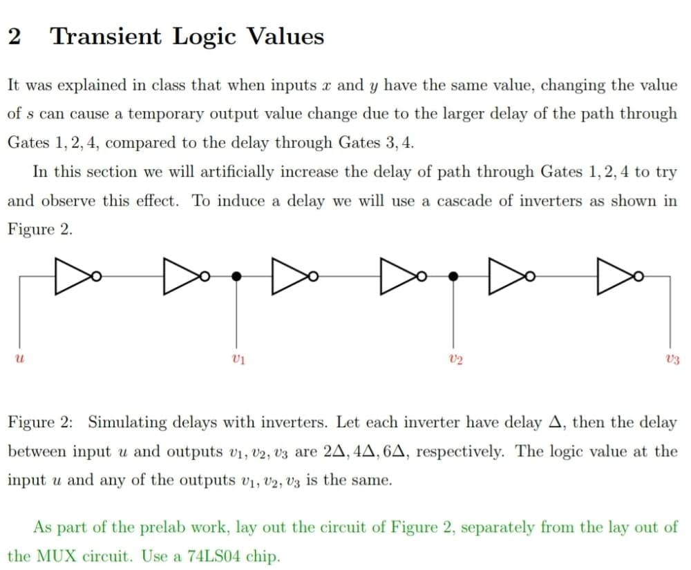
It was explained in class that when inputs x and y have the same value, changing the value
of s can cause a temporary output value change due to the larger delay of the path through
Gates 1, 2, 4, compared to the delay through Gates 3, 4.
In this section we will artificially increase the delay of path through Gates 1,2, 4 to try
and observe this effect. To induce a delay we will use a cascade of inverters as shown in
Figure 2.
vị
V2
V3
Figure 2: Simulating delays with inverters. Let each inverter have delay A, then the delay
between input u and outputs v1, v2, V3 are 2A, 4A, 6A, respectively. The logic value at the
input u and any of the outputs v1, v2, V3 is the same.
As part of the prelab work, lay out the circuit of Figure 2, separately from the lay out of
the MUX circuit. Use a 74LS04 chip.
Expert Solution
This question has been solved!
Explore an expertly crafted, step-by-step solution for a thorough understanding of key concepts.

Step by step
Solved in 2 steps with 3 images

Knowledge Booster


Learn more about
Need a deep-dive on the concept behind this application? Look no further. Learn more about this topic, electrical-engineering and related others by exploring similar questions and additional content below.Recommended textbooks for you