Draw the electronic circuit of a subtraction amplifier with two inputs (V. and V2) and one output (V.) implemented using only one operational amplifier. Substitute the equation that gives V. in terms of Vi and V2 using circuit analysis techniques. DO NOT use any pre-driven formula and consider the amplifier is an ideal one.
Q: Identify any FOUR assumptions commonly made in the analysis of operational amplifier circuits,…
A: Note: We are authorized to answer one question at a time since you have not mentioned which question…
Q: 7. An amplifier has a gain of 36,000, which is to0 big value for application. If we give T0uV the…
A: An amplifier amplifies a given signal. It is done so to process the input signal well. Operational…
Q: 1. In a capacitively coupled amplifier, the input coupling capacitor and the output coupling capac-…
A:
Q: a) As an electronics engineer, you are given a task to design power amplifier using the Bipolar…
A: Note: We are authorized to answer one question at a time since you have not mentioned which question…
Q: Provide any three of the characteristics of ideal operational amplifiers. the following operational…
A: Characterstics of ideal opamp: Infinite open loop voltage gain Infinite input impedance Zero output…
Q: Figure 6 shows a circuit where feedback is provided between the drain and gate of the transistor M1…
A: “Since you have posted a question with multiple sub-parts, we will solve first three subparts for…
Q: pVcc = 15V 2.2kN 2.2kN 15KN 15KN 10μF o Vo Q2 10µF 10μF 4.7kN, : 20μ F 4.7kN 1kN 1kN - 20μF
A: (a) Here, while doing the dc analysis of the given circuit, all the capacitors become…
Q: A Design an inverting amplifier to provide a closed-loop voltage gain of Ay = -22 V/V. The maximum…
A:
Q: For the amplifier shown below, the ideal Vou VS. Vin characteristic has been plotted. However,…
A:
Q: Find the gain (Vout / Vin) of the circuit below. Note: VB voltage source is a DC source and do not…
A: Small-signal modeling of the given amplifier will be Now the impedance offered by load 3 will be…
Q: Shown is an ideal operational amplifier with Voltage V1 connected to its non-inverting input. What…
A: Find the output voltage of the given ideal operational amplifier ?
Q: P9.8. Given that the amplifiers having the characteristics shoWr are cascaded in the order A - B,…
A:
Q: Write the characteristics of operational amplifier. Don't write in the paper and take picture
A: In this question, We are going to define the characteristics of operational amplifier.
Q: What approximations are valid for the voltages and currents shown in the figure of an ideal…
A:
Q: From these data in Table, compute the gains Ad and Acm and verify that they are as designed. (Q2)…
A: “Since you have asked multiple questions, we will solve the first question for you. If you want any…
Q: Syeda and Urmi are two friends who are doing a class in the course of Electrical Drives and…
A: The full form of CMRR is Common Mode Rejection Ratio. CMRR is defined as the ratio of differential…
Q: In a capacitively coupled amplifier, the input coupling capacitor and the output coupling capac-…
A: Capacitor:- Capacitor stores electrical charges in electric field. Capacitance is the effect of…
Q: Derive an expression for non inverting amplifier and determine its gain.
A: Given: Non-inverting amplifier:
Q: Operational amplifier (Op-Amp) Exercise In a certain application, a signal source having 60 kn of…
A: Solution : Note : In this question they have given an option between the inverting and…
Q: IkN Vị o Vo 2k£2 DEAL Rf 3kN
A:
Q: Draw the circuit of 3 op-amp configuration of instrumentation amplifier and derive the gain…
A: The circuit of a 3 op-amp configuration of instrumentation amplifier can be drawn as:
Q: Your Boss asks you to get more knowledge about operational amplifiers by studying specific…
A: Solution(A)- 1. We will select BC 547 for BJT - The pin diagram of BC 547 and specifications are…
Q: Assume an operational amplifier is working on inverting amplifier in which it takes input resistance…
A: Given that Ri=30ΩRf=60ΩVi=150volt
Q: We can make use of a non-inverting amplifier to build a -current source. To do this, consider the…
A:
Q: A noninverting amplifier is designed to have a gain of 200 (46 dB) and is built using an operational…
A: Given data, The value of gain 1β = 200. The value of open loop gain is A= 80 dB. Converting open…
Q: 2) The circuit below shows a circuit for a differential amplifier with an active load. Here Q1 and…
A:
Q: Non-inverting amplifier is designed to provide an amplified signal which is in phase with the signal…
A:
Q: A Design an inverting amplifier to provide a closed-loop voltage gain of Ay = -22 V/V. The maximum…
A:
Q: R₁ www Vout + Vin For the operational amplifier circuit shown, what value must R2 be in kilohms in…
A: The solution is given below.
Q: What is the required value of ? for a voltage gain of 10 b) Determine ?out
A:
Q: Consider an amplifier operating from +10-V power supplies. It is fed with a sinusoidal voltage…
A: Amplifier is an electronic device whose output is amplified version of the input signal. The…
Q: Note that V1 and V2 are ac voltage sources. In the circuit shown, assume transistors are matched and…
A: Given the amplifier: We need to find: a) Differential mode gain b) Common mode gain c) CMRR…
Q: Exercise 1-4: In a certain application, a signal source having 60 k2 of source impedance, Rs.…
A:
Q: Design a feedback amplifier with a de gain of 10 V N and a 3-dB bandwidth of at least IO MHz. The…
A: Given: The feedback amplifier is having a gain of 10 V/V and a 3-dB bandwidth of at least 10 MHz.…
Q: Suppose we have a resistive load that varies from 5 kΩ to 10 kΩ .We connect this load to an…
A: Given: To find the parameter of the amplifier is important in this situation and range of values is…
Q: Given values - β is 100 Vth =0.4 Calculate the gain of the following amplifiers. Use appropriate…
A: We have given the problem Calculate the gain of the following amplifiers. Use appropriate…
Q: An ECE 2010 student does not believe into the magic of the negative feedback (2nd SPC). Instead,…
A:
Q: Outline the main features of a non-inverting operational amplifier
A: Features of a non inverting operational amplifier
Q: Explain the principle of operation and the type of feedback for the op-amp in the circuit in (D).…
A: An amplifier is an electronic device that amplifies the input signal given into it and gives the…
Q: The inverting amplifier in the circuit shown has an input resistance of 500 K ? an output resistance…
A: For inverting amplifier in the question ; Give data A=Gain=300,000Ri=Input resistance=500…
Q: A single-transistor amplifier is needed that has a gain of approximately 66 dB and an input…
A: Given: Gain = 66 dB Input resistance = 250 kΩ
Q: 4. Is it possible to get a gain less than unity using a non-inverting amplifier configuration? If…
A: No it is not possible
Q: 1.Syeda and Urmi are two friends who are doing a class in the course of Electrical Drives and…
A: Amplifiers are used to provide the amplified signal of the input signal. In a mic speaker setup, the…
Q: Suppose we have a two-stage cascaded amplifier with an ideal transconductance amplifier as the first…
A: a) The two-stage cascaded amplifier is shown below,
Q: Identify any FOUR assumptions commonly made in the analysis of operational amplifier circuits,…
A: Note: We are authorized to answer one question at a time since you have not mentioned which question…
Q: Given values - β is 100 Vth =0.4 Calculate the gain of the following amplifiers. Use appropriate…
A:
Q: Given in the figure is a two-stage amplifier design that employs negative feedback. Answer the…
A: Given the circuit, as shown below: Given in the figure is a two-stage amplifier design that employs…
Q: Design a series Fed Class A amplifier using a silicon transistor with beta value 25 which gives…
A: Since you have asked multiple questions, we will solve the first question for you. If you want any…
Q: ) Below is the small signal model of a multistage amplifier. Using this mo del, write the…
A: Given circuit of multistage amplifier
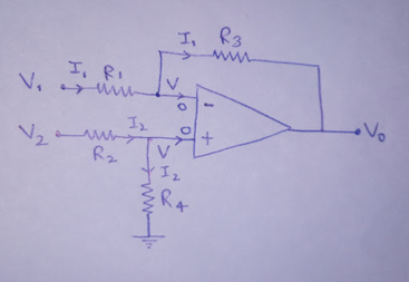
Draw the electronics circuit of the subtraction amplifier or differential amplifier, with two inputs and one output and using one op-amp.
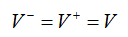
As the op-amp is ideal, no current flows through it.
Write the expression for voltage V.
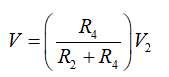
Also, the ideal op-amp exhibits the characteristics of the virtual ground.
Write the expression for the node voltage of op-amp.
Step by step
Solved in 4 steps with 5 images
- What approximations are valid for the voltages and currents shown in the figure of an ideal operational amplifier. What conditions must be satisfied for these approximations?Suppose we have a two-stage cascaded amplifier with an ideal transconductance amplifier as the first stage and an ideal transresistance amplifier as the second stage. What type of amplifier results and what is its gain in terms of the gains of the two stages? Repeat for the amplifiers cascaded in the opposite order.Slove Foperational amplifiers of your choice both FET and BJT based technologyA) From the datasheet, find the number of pins of the Op-amp IC, the open-loop gain,bandwidth, CMRR, slew rate, Voltage offset, current offset, input and output impedance,recommended supply voltages. Tabulate your outcomes with evidence from the data sheets.For both types of Op-Amps. Discus advantages and disadvantages of both.B) Mention available amplifiers that this op-amp is used for and discuss in brief itsapplications.C) Build a simple differentiator circuit, having C=1µF and R = 1kΩ for the op-amp chosen in(A), virtual using Multisim. Evaluate the voltage saturation, compare your findings with bothtypes of op-amps (FET and BJT) and analyze briefly how you concluded your result.D) Build a simple non-inverting amplifier with a gain of 10V/V circuit, using the op-ampchosen in (A) either BJT or FET, virtual using Multisim. Evaluate the slew rate, and theamplifier specification in terms of conduction angle…
- Outline the main features of a non-inverting operational amplifierGiven in the figure is a two-stage amplifier design that employs negative feedback. Answer the following questions. Use the notation (R1 + R2 + ... + Rn) for series resistors and (R1 || R2 || ... || Rn) for parallel resistors for clarity and ease. Assume that the transistors are already biased properly in the saturation region and ro1 = ro2 → ∞. Also assume that the capacitors have infinite capacitance. 1.) Find the expression for the open loop gain Av 2.) Derive the resistance Rin which is the resistance that can be seen at the input port of the amplifierSuppose we have a resistive load that varies from 5 kΩ to 10 kΩ .We connect this load to an amplifier, and we need the voltage across the load to vary by less than 1 percent with variations in the load resistance. What parameter of the amplifier is important in this situation? What range of values is allowed for the parameter?
- Identify an industrial application where MULTISTAGE AMPLIFIER is required and design circuit for the same application and Draw the appropriate circuit diagram, functioning diagram.Assume for a moment that perfectly accurate resistors were available for feedback networks; that is resistor tolerance is 0%. Then any deviation from the value set by the feedback resistor ratio is caused by insufficient raw op-amp gain. What minimum raw gain would be needed to get within 1% if an intended overall gain of 10? What if the intended gain is 100 instead?An amplifier is formed by cascading two operational-amplifier stages, as shown (a). (a) Replace each amplifier stage with its two-port representation. (b) Use the circuit model from part (a) to find the overall two-port representation (Av, Rin, Rout) for the complete twostageamplifier. (c) Draw the circuit of the two-port corresponding to the complete two-stage amplifier.
- Question 3: Please write answers to all parts of the question in the separate dot points as shown What is the circuit called? Discuss all components including voltage sources. Which components determine the closed-loop gain of the circuit? Describe the slew-rate of the op-amp. Describe the Common-Mode-Rejection ratio of the op-amp? What is the unity gain bandwidth? Describe the gain bandwidth product (GBP). Describe the GBP relationship between the break (critical) frequency and the gain? What two methods calculate the max frequency? If one produces a higher value of maximum frequency than the other, which would you use as the maximum frequency?We examined the common source amplifier shown in the figure in the 5th experiment. The capacitances have high enough value to assume them short circuit for the small-signal conditions. The gain of the amplifier for no-load condition is measured as 60. When a load resistance RL = 13 kΩ is connected, the gain is measured as 10. Calculate the output impedance of the amplifier, Rout.Suppose the output signal voltage from the amplifier is 35 times the input signal voltage. If the imput and output impedance are both pure resistances of the same value, what is the gain