Draw the small-signal equivalent circuit of the complete amplifier and perform an ac analysis to show that the approximate overall small-signal voltage gain is given by the expression; vo A, = - Im1(Rc || R1) = Assume ß1 = B2= ß = 150, VBE1(active) = V BE2(active) = Vbe(active) = 0.7 V, VAI= VA= VA= 0, VT = 26 mV, and Vcc= 15 V.
Draw the small-signal equivalent circuit of the complete amplifier and perform an ac analysis to show that the approximate overall small-signal voltage gain is given by the expression; vo A, = - Im1(Rc || R1) = Assume ß1 = B2= ß = 150, VBE1(active) = V BE2(active) = Vbe(active) = 0.7 V, VAI= VA= VA= 0, VT = 26 mV, and Vcc= 15 V.

Power System Analysis and Design (MindTap Course List)
6th Edition
ISBN:9781305632134
Author:J. Duncan Glover, Thomas Overbye, Mulukutla S. Sarma
Publisher:J. Duncan Glover, Thomas Overbye, Mulukutla S. Sarma
Chapter12: Power System Controls
Section: Chapter Questions
Problem 12.3P

Related questions
Question
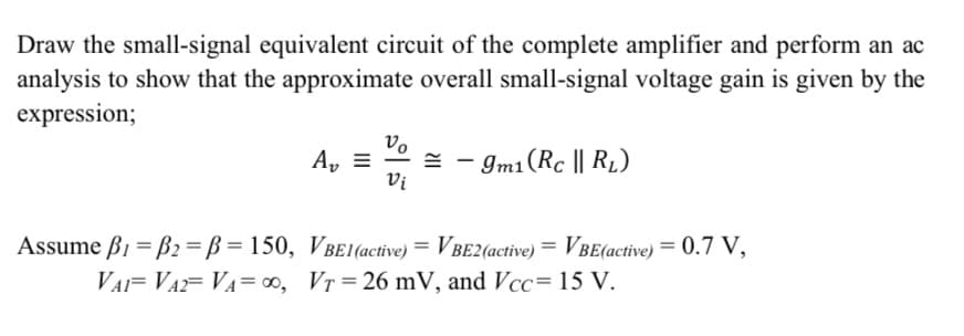
Transcribed Image Text:Draw the small-signal equivalent circuit of the complete amplifier and perform an ac
analysis to show that the approximate overall small-signal voltage gain is given by the
expression;
vo
= - Im1(Rc || R1)
Vi
A, =
Assume ß1 = B2 = B = 150, VBe1(active) = VBe2(active) = VBe(active) = 0.7 V,
VAF VA= VA= ∞, Vr = 26 mV, and Vcc= 15 V.
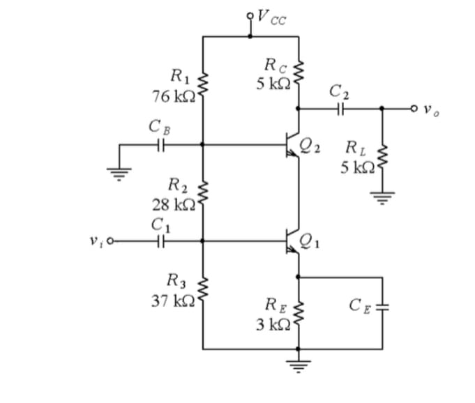
Transcribed Image Text:Rc
5 kN
R1
C2
76 kQ
Vo
CB
Q2 RL
5 kN
R2
28 kQ'
C1
R3
37 k2
CE
RE Z
3 kQ
Expert Solution
This question has been solved!
Explore an expertly crafted, step-by-step solution for a thorough understanding of key concepts.

Step by step
Solved in 2 steps with 1 images

Knowledge Booster


Learn more about
Need a deep-dive on the concept behind this application? Look no further. Learn more about this topic, electrical-engineering and related others by exploring similar questions and additional content below.Recommended textbooks for you
Power System Analysis and Design (MindTap Course …
Electrical Engineering
ISBN:
9781305632134
Author:
J. Duncan Glover, Thomas Overbye, Mulukutla S. Sarma
Publisher:
Cengage Learning
Power System Analysis and Design (MindTap Course …
Electrical Engineering
ISBN:
9781305632134
Author:
J. Duncan Glover, Thomas Overbye, Mulukutla S. Sarma
Publisher:
Cengage Learning