Fill in the empty cells within the table below with increase (†), decrease (↓), or no change (→) for a MOSFET device. (Consider NMOS for simplicity)
Fill in the empty cells within the table below with increase (†), decrease (↓), or no change (→) for a MOSFET device. (Consider NMOS for simplicity)

Introductory Circuit Analysis (13th Edition)
13th Edition
ISBN:9780133923605
Author:Robert L. Boylestad
Publisher:Robert L. Boylestad
Chapter1: Introduction
Section: Chapter Questions
Problem 1P: Visit your local library (at school or home) and describe the extent to which it provides literature...

Related questions
Question
Use charts if needed
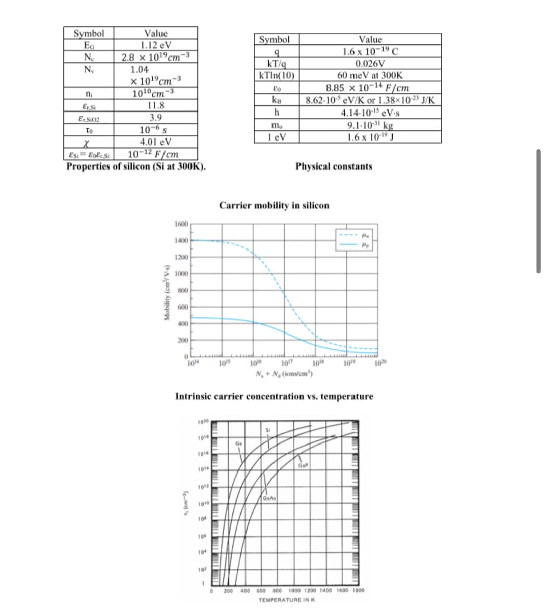
Transcribed Image Text:Symbol
EG
Ne
Ny
n₁
Er Si
Er,SiO2
To
X
Value
1.12 eV
2.8 x 1019 cm-3
1.04
x 101⁹ cm-3
10¹0 cm-3
11.8
3.9
10-6 s
4.01 eV
Esi Eger,Si
10-12 F/cm
Properties of silicon (Si at 300K).
Mobility (cm²/V-s)
1600
1400
1200
1000
800
600
400
200
0
1014
(a)
1020
1018
1016
1014
1012
1010
1016 1017 10
N₂ + N₂ (ions/cm³)
Intrinsic carrier concentration vs. temperature
10⁰
104
10⁰
10²
Symbol
q
kT/q
KTIn(10)
Eo
KB
h
1015
mo
1 eV
Ge
Carrier mobility in silicon
0.026V
60 meV at 300K
8.85 × 10-¹4 F/cm
8.62-105 eV/K or 1.38×10⁻²³ J/K
GaAs
Value
1.6 x 10⁻¹⁹ C
Physical constants
www
4.14-10-15 eV-s
9.1-10-31 kg
1.6 x 10⁻¹⁹ J
GaP
Ha
1019 10
1
0 200 400 600 800 1000 1200 1400 1600 1800
TEMPERATURE IN K
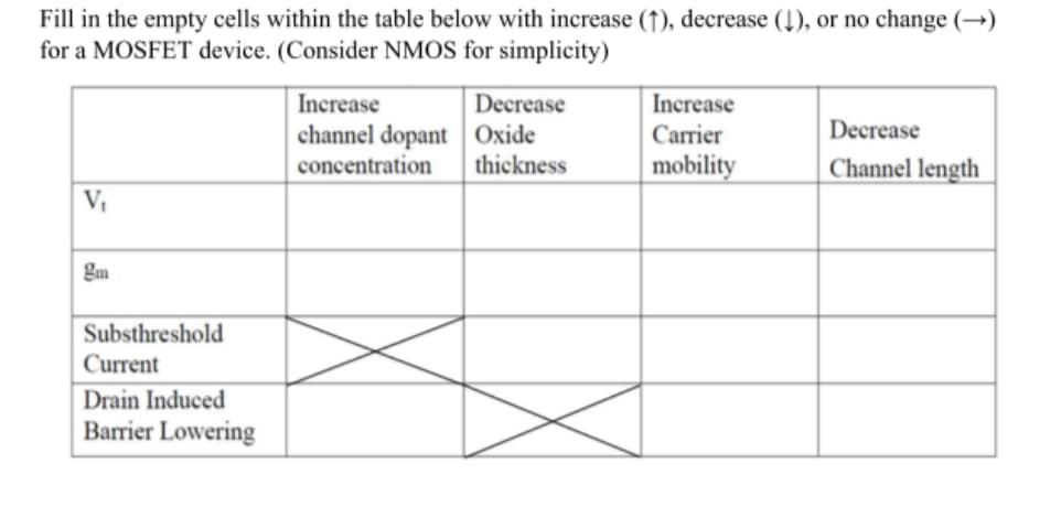
Transcribed Image Text:Fill in the empty cells within the table below with increase (1), decrease (1), or no change (→)
for a MOSFET device. (Consider NMOS for simplicity)
V₁
gm
Substhreshold
Current
Drain Induced
Barrier Lowering
Increase
channel dopant
Decrease
Oxide
concentration thickness
Increase
Carrier
mobility
Decrease
Channel length
Expert Solution
This question has been solved!
Explore an expertly crafted, step-by-step solution for a thorough understanding of key concepts.

Step by step
Solved in 5 steps with 3 images

Knowledge Booster


Learn more about
Need a deep-dive on the concept behind this application? Look no further. Learn more about this topic, electrical-engineering and related others by exploring similar questions and additional content below.Recommended textbooks for you
Introductory Circuit Analysis (13th Edition)
Electrical Engineering
ISBN:
9780133923605
Author:
Robert L. Boylestad
Publisher:
PEARSON

Delmar's Standard Textbook Of Electricity
Electrical Engineering
ISBN:
9781337900348
Author:
Stephen L. Herman
Publisher:
Cengage Learning

Programmable Logic Controllers
Electrical Engineering
ISBN:
9780073373843
Author:
Frank D. Petruzella
Publisher:
McGraw-Hill Education
Introductory Circuit Analysis (13th Edition)
Electrical Engineering
ISBN:
9780133923605
Author:
Robert L. Boylestad
Publisher:
PEARSON
Delmar's Standard Textbook Of Electricity
Electrical Engineering
ISBN:
9781337900348
Author:
Stephen L. Herman
Publisher:
Cengage Learning
Programmable Logic Controllers
Electrical Engineering
ISBN:
9780073373843
Author:
Frank D. Petruzella
Publisher:
McGraw-Hill Education

Fundamentals of Electric Circuits
Electrical Engineering
ISBN:
9780078028229
Author:
Charles K Alexander, Matthew Sadiku
Publisher:
McGraw-Hill Education

Electric Circuits. (11th Edition)
Electrical Engineering
ISBN:
9780134746968
Author:
James W. Nilsson, Susan Riedel
Publisher:
PEARSON

Engineering Electromagnetics
Electrical Engineering
ISBN:
9780078028151
Author:
Hayt, William H. (william Hart), Jr, BUCK, John A.
Publisher:
Mcgraw-hill Education,