For the Differential amplifier shown:, calculate the following: 1. The differential mode gain 2. Input resistance 3. Output resistance Given: Kı=K2=100µA/V² • K=K=Ks=K=K=200µA/V? • Rref-40k2 • VAp-50V, VAn=100V |Vrl= Vra =2V +5V M3 М4
For the Differential amplifier shown:, calculate the following: 1. The differential mode gain 2. Input resistance 3. Output resistance Given: Kı=K2=100µA/V² • K=K=Ks=K=K=200µA/V? • Rref-40k2 • VAp-50V, VAn=100V |Vrl= Vra =2V +5V M3 М4

Power System Analysis and Design (MindTap Course List)
6th Edition
ISBN:9781305632134
Author:J. Duncan Glover, Thomas Overbye, Mulukutla S. Sarma
Publisher:J. Duncan Glover, Thomas Overbye, Mulukutla S. Sarma
Chapter12: Power System Controls
Section: Chapter Questions
Problem 12.3P

Related questions
Question
please solve this asap
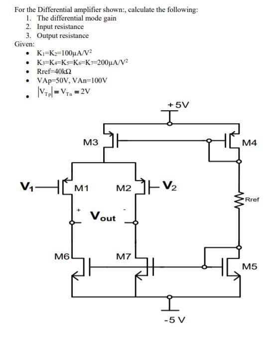
Transcribed Image Text:For the Differential amplifier shown:, calculate the following:
1. The differential mode gain
2. Input resistance
3. Output resistance
Given:
• K=K2=100µA/V?
• K=K=Ks=K6=K7=200µA/V?
• Rref-40k2
• VAp-50V, VAn=100V
Vr =Vra = 2V
Tn
+5V
M3
M4
V
HM1
M2 JEV2
Rref
Vout
M6
M7
M5
-5 V
Expert Solution
This question has been solved!
Explore an expertly crafted, step-by-step solution for a thorough understanding of key concepts.

Step by step
Solved in 2 steps with 1 images

Knowledge Booster


Learn more about
Need a deep-dive on the concept behind this application? Look no further. Learn more about this topic, electrical-engineering and related others by exploring similar questions and additional content below.Recommended textbooks for you
Power System Analysis and Design (MindTap Course …
Electrical Engineering
ISBN:
9781305632134
Author:
J. Duncan Glover, Thomas Overbye, Mulukutla S. Sarma
Publisher:
Cengage Learning
Power System Analysis and Design (MindTap Course …
Electrical Engineering
ISBN:
9781305632134
Author:
J. Duncan Glover, Thomas Overbye, Mulukutla S. Sarma
Publisher:
Cengage Learning