Identify the memory IC shown to the right: a) What is it: Microprocessor/Cache Memory/SRAM/DRAM/EPROM Vcc 24 Vss 23 D3 22 D2 21 CAS 20 OE 19 A9 184 b) How many addressable locations it has DO 2 D1 3 WE 14 RAS NC 6 A10 7 A0 S AS A1 19 A2 10 A3 11 1기 A7 16 A6 15 AS 144 13 A4 Vce 12 Vss Top View
Identify the memory IC shown to the right: a) What is it: Microprocessor/Cache Memory/SRAM/DRAM/EPROM Vcc 24 Vss 23 D3 22 D2 21 CAS 20 OE 19 A9 184 b) How many addressable locations it has DO 2 D1 3 WE 14 RAS NC 6 A10 7 A0 S AS A1 19 A2 10 A3 11 1기 A7 16 A6 15 AS 144 13 A4 Vce 12 Vss Top View

Chapter22: Sequence Control
Section: Chapter Questions
Problem 6SQ: Draw a symbol for a solid-state logic element AND.

Related questions

Question
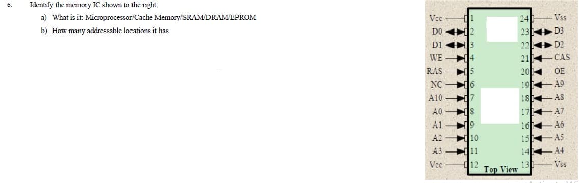
Transcribed Image Text:6.
Identify the memory IC shown to the right:
a) What is it: Microprocessor/Cache Memory/SRAM/DRAM/EPROM
Vcc
24
Vss
23 D3
22 D2
b) How many addressable locations it has
DO 12
D1 3
WE 14
21 CAS
20 OE
19 49
18 AS
RAS
i15
NC 6
A10 7
17 A7
16 46
15 AS
A0 IS
A1 게9
A2 10
A3 11
14 4
13 Vss
Vce
d12
Top View
Expert Solution
This question has been solved!
Explore an expertly crafted, step-by-step solution for a thorough understanding of key concepts.

Step by step
Solved in 2 steps with 1 images

Knowledge Booster


Learn more about
Need a deep-dive on the concept behind this application? Look no further. Learn more about this topic, electrical-engineering and related others by exploring similar questions and additional content below.Recommended textbooks for you