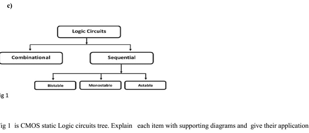
is CMOS static Logic circuits tree. Explain each item with supporting diagrams and give their application


Q: Briefly describe the internal and external control of inverters.
A: The meaning of control of the inverter is to control the output voltage of the inverter. The output…
Q: PROBLEM# 2:55 1 Design the simpliest CMOS logic circuit to implement (ABC) + D. How many transistors…
A:
Q: Figure shows a design for an inverting bus driver that achieves the same effect as a tri-state…
A:
Q: This guestion considers the logic function f(a,b,c,d) = (a+b+c)•d. %3D (a) Design and draw a custom…
A: The logic function is given below, fa,b,c,d = a+b+c·d¯
Q: a) One extremely powerful aspect of CMOS is the ability to create single gate circuits that can…
A: CMOS is complementary circuit. It have two pairs of complementary circuits. One is NMOS circuit and…
Q: 3) Consider the CMOS logic gate that implements the function Y = C + BD + CBA a) Draw the circuit…
A: Given: The CMOS logic gate that implements the function: Y=C+BD+C¯BA To find: a) Draw the circuit…
Q: how CMOS transistors circuits can be used to implement binary information and digital logic. Explain…
A: Information is saved on the pc in binary form. A binary bit can exist in one among possible states.…
Q: We need to implement digital logic function Y A(B +C(D+ E)). %3D a) Design a CMOS logic gate to…
A:
Q: Introduce CMOS Logic Gates in steps?
A:
Q: Design a CMOS logic gate that implements the logic function Y (CD+ A)B + F if the reference inverter…
A:
Q: explain in your own words the principle of PUN and PDN with respect to static logic circuit…
A: Static CMOS is the extension of the static CMOS inverter to multiple inputs. A static CMOS gate is a…
Q: Design and draw the circuits below at flip-flop level. a) A 3-bit synchronous binary counter with…
A:
Q: For a CMOS logic gate circuit given below a.) Sketch and Label the types of MOSFET for Ml, M2, M3,…
A: According to the bartleby's guidelines we have to solve only first three subparts of a question so…
Q: (d) Draw the folowing Boolean expression using CMOS transistors. (i) Y = AD + AE + BC. (ii) Y = ACD…
A:
Q: 2. Draw the static CMOS schematic to implement the Boolean function F = (A+B)(C+D)
A:
Q: In a device that follows CMOS logic protocol, the power supply is +15 V. The state is considered…
A: A digital logic operates at two voltage levels. They are Logic '1' or high and Logic '0' or low.…
Q: Designing A 4 Bit Operation Arithmetic Logic Unit
A: Arithmetic Logic Unit is a common operational unit with number of storage registers connected to it,…
Q: A waveform is applied to an inverter in Figure corresponding to the input and show the timing…
A: An AND gate is a logic gate whose output is high only if all of the input is High. OR gate is a…
Q: Identify the correct statement with respect to CMOS logic family a. Integrates NPN transistors and…
A:
Q: a) Sketch the schematic of a 2 input XOR gate in Cascode Voltage Switch Logic (CVSL). b) Sketch the…
A: “Since you have asked multiple questions, we will solve the first question for you. If you want any…
Q: 5) Design a CMOS logic gate that implements the logic function Y= A(BC + DE) and is twice as fast as…
A: CMOS logic circuit- They are made up of MOSFET used to perform logic function. These are used for…
Q: Using a table, compare the characteristics (basic gate(positive logic), fan-out, power dissipation…
A: Here we need to compare the characteristics Such as basic gate, noise Immunity, propagation delay…
Q: What are the basic logic gates in the MOS logic family?
A: In this case, the correct option corresponding to the basic logic gates in the MOS logic family is…
Q: One extremely powerful aspect of CMOS is the ability to create single gate circuits that can…
A: We need to implement the function Y=A+{B×(C+D)} using CMOS. CMOS is a circuit consisting of both…
Q: 4) Draw a logic diagram of a divide-by-14 counter using IC 7493 and 2-input AND gate.
A: Circuit diagram of inside the IC 7493 is as shown below:
Q: Explore layout of CMOS inverters and logic gates.
A: The circuit of CMOS inverter is made with one nMOS and one pMOS transistor. but the combinations…
Q: Identify the correct statement with respect to CMOS logic family O a. High power dissipation O b.…
A: In CMOS logic family,
Q: Design Master-Slave Flip Flop circuit diagram and write a short description.
A: Race around Condition- One time duration which is a large number of toggle on and off which is…
Q: 1. (a) Implement the logic function F = {A(BC + D)}' using a 4-input static CMOS logic gate using…
A:
Q: Q3) Design a 4-bit even parity generator circuit using: а. Basic logic gates. b. Decoder IC.
A: As per our guidelines we are supposed to answer only one question. Kindly repost other questions as…
Q: Which of the following is correct regarding the comparison between TTL and CMOS? >CMOS design is…
A:
Q: CMOS with a PDP of 50 fJ is to be used in a chipdesign that requires 100 million gates. The chip…
A: Given: To find the minimum logic gate delay that can be used in the design if all the gates operate…
Q: ) Describe, with the help of sketches, the definition and meaning of noise margins in an inverter…
A: The noise margin is the proportion of noises that a logic circuit can hold out against. Noise margin…
Q: Q7 Design a CMOS logic layout for the following function: F= (A.B+C)+C+D
A:
Q: Consider the following digital logic circuit: OR AND NOT AND R Give the Boolean expression that…
A:
Q: Implement the following logic function using complementary CMOS. a) Y = ((Ā + B) ·(Č +D+ E) + F) · G…
A:
Q: Implement the following function using 4-input CMOS gate and an inverter? (A+B) (C+D)
A: Given inputs to the CMOS gate are A, B, C, and D We have to implement the function F=A+BC+D using…
Q: DESIGN A CIRCUIT THAT ADDS AN 8-BIT BINARY NUMBER TO ANOTHER 8-BIT BINARY NUMBER USING THE IC 74283…
A:
Q: A Bo o -AO121(A,B,C) Co Figure 4.2: The AOI21 operation
A: Digital electronics problem . Below is the explaination:-
Q: Explore sources of static and dynamic power dissipation in CMOS logic.
A: CMOS refers to "Complementary Metal Oxide Semiconductor" . They are made of silicon and germanium,…
Q: Describe and compare the characteristics of TTL and CMOS Logic families. Please don't write on paper
A: FIND: Compare characteristics of TTL and CMOS logic families
Q: a) For the logic function f a. (b + c), using CMOS concept draw the stick diagram and write the pull…
A: Here we need to design the given logic function using CMOS. The generalized block diagram will be
Q: Define Combined (Combinational) and Extraordinary (Sequential) Logic circuits with the figure,…
A: Combinational circuits are portrayed as the time free circuits which don't depends on past…
Q: (a) Construct an Inverter Logic Gate using both TTL and CMOS Logic Family.
A:
Q: 4. Consider the circuit below on the left. a) What logic function does it perform? (What is F in…
A: CMOS When connected to a common secondary voltage, a complementary metal-oxide-semiconductor is made…
Q: One extremely powerful aspect of CMOS is the ability to create single gate circuits that can…
A: Please find the details solution in below images

Step by step
Solved in 4 steps with 5 images


- In designing static CMOS Logic circuits a principle of pull –up networks and pull- down networks is applied . Explain in your own understanding how this principle works2(MCQ). The Logic Expression for the following CMOS circuit is: a. shown in image b. shown in image c. shown in image d. shown in imageDescribe and compare the characteristics of TTL and CMOS Logic families. Please don't write on paper
- a) Static logic circuit is a design methodology in integrated circuit design where there is at all times some mechanism to drive the output either high or low. A static CMOS gate is a combination of two networks, called the pull-up network (PUN) and the pull- down network (PDN). With the back ground stated , explain in your own words the principle of PUN and PDN with respect to static logic circuit formationWith necessary diagrams and equations, describe the operations of single-phase half-bridge and full-bridge inverters. Briefly describe the internal and external control of inverters.Introduce CMOS Logic Gates in steps?
- One extremely powerful aspect of CMOS is the ability to create single gate circuits that can implement functions consisting of several basic Boolean logic operations. This makes digital CMOS design quite different from classical logic design techniques, since now the logic expressions and the corresponding circuits become very closely related. With this back ground how would you solve Y = A +{ B × ( C +D ) } using what you have learnedHow would you manipulate this equation to get it into a format where you can draw it as a NAND and inverter gates logic diagram and a NOR and inverter gates logic diagram?Sketch the schematic of z in pseudo nmos logic