lean algebra to simplify the following expression, then draw a logic gate circuit for the simpli AB+ABC ABC ABC algebra to simplify the following logic gate circuit DDD A B algebra to simplify the following logic gate circuit: :DD A B Output Output
lean algebra to simplify the following expression, then draw a logic gate circuit for the simpli AB+ABC ABC ABC algebra to simplify the following logic gate circuit DDD A B algebra to simplify the following logic gate circuit: :DD A B Output Output

Chapter22: Sequence Control
Section: Chapter Questions
Problem 6SQ: Draw a symbol for a solid-state logic element AND.

Related questions
Question
Plz answer question 13
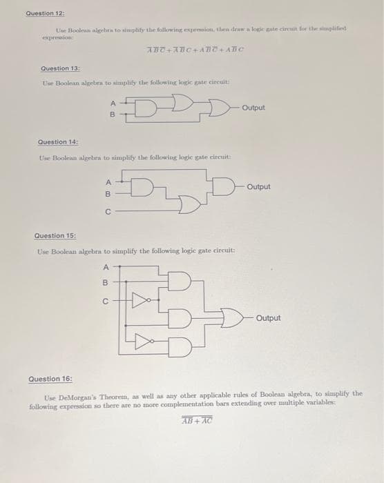
Transcribed Image Text:Question 12:
Use Boolean algebra to simplify the following expression, then draw a logic gate circuit for the simplified)
expression
Question 13:
Use Boolean algebra to simplify the following logic gate circuit:
Question 14:
Question 15:
Use Boolean algebra to simplify the following logic gate circuit:
D
A
B
Question 16:
A
B
с
ABC+ABC+ABC+ABC
Use Boolean algebra to simplify the following logic gate circuit:
AB
C
Output
Output
Output
Use DeMorgan's Theorem, as well as any other applicable rules of Boolean algebra, to simplify the
following expression so there are no more complementation bars extending over multiple variables:
AB+AC
Expert Solution
This question has been solved!
Explore an expertly crafted, step-by-step solution for a thorough understanding of key concepts.

This is a popular solution!

Trending now
This is a popular solution!

Step by step
Solved in 2 steps with 2 images

Knowledge Booster


Learn more about
Need a deep-dive on the concept behind this application? Look no further. Learn more about this topic, electrical-engineering and related others by exploring similar questions and additional content below.Recommended textbooks for you