OR gate to generate the output. For circuit 1, X is defined to be 1 if and only if the binary representation of A, B, C and D is even. Note A is the most significant bit, then B, then C, and D is the least significant. For circuit 2, X is defined to be 1 if and only if the total number of 1's among A, B, C and D is even. Which of the following 4-input gates would be used in the implementation of both circuits? D TIYT
OR gate to generate the output. For circuit 1, X is defined to be 1 if and only if the binary representation of A, B, C and D is even. Note A is the most significant bit, then B, then C, and D is the least significant. For circuit 2, X is defined to be 1 if and only if the total number of 1's among A, B, C and D is even. Which of the following 4-input gates would be used in the implementation of both circuits? D TIYT

Chapter22: Sequence Control
Section: Chapter Questions
Problem 6SQ: Draw a symbol for a solid-state logic element AND.

Related questions
Question
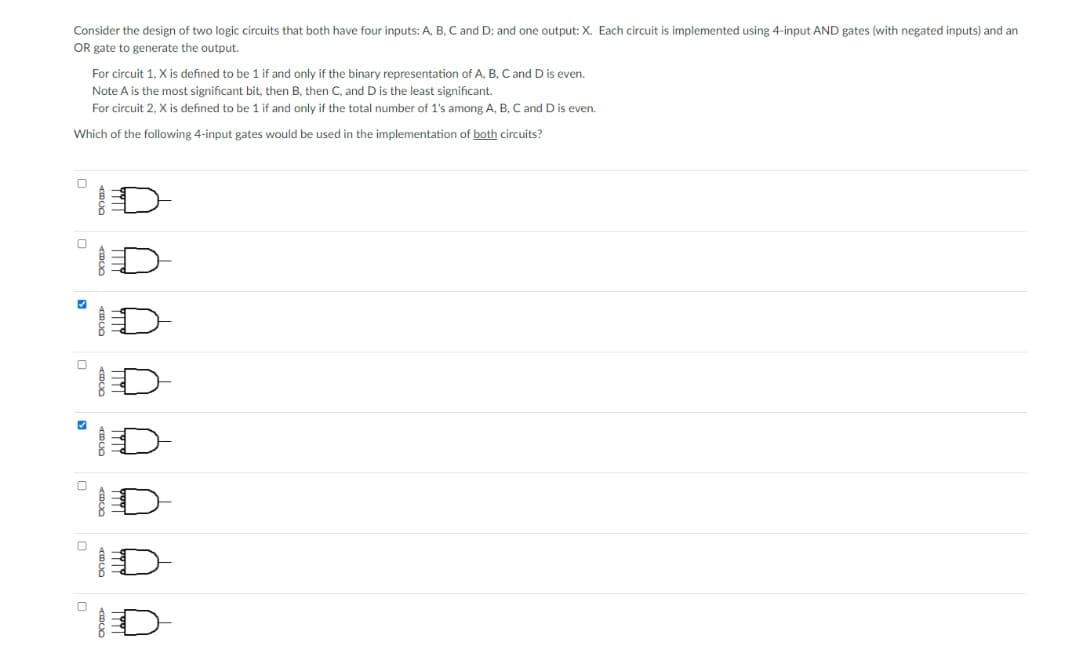
Transcribed Image Text:Consider the design of two logic circuits that both have four inputs: A, B, C and D; and one output: X. Each circuit is implemented using 4-input AND gates (with negated inputs) and an
OR gate to generate the output.
For circuit 1, X is defined to be 1 if and only if the binary representation of A, B, C and D is even.
Note A is the most significant bit, then B, then C, and Dis the least significant.
For circuit 2, X is defined to be 1 if and only if the total number of 1's among A, B, C and D is even.
Which of the following 4-input gates would be used in the implementation of both circuits?
Expert Solution
This question has been solved!
Explore an expertly crafted, step-by-step solution for a thorough understanding of key concepts.

This is a popular solution!

Trending now
This is a popular solution!

Step by step
Solved in 2 steps

Recommended textbooks for you