Part I: Amplifier Specifications. • Use no more than three 2N3904 transistors. • The overall amplifier gain should be at least A, = +50 • Input signal should be Vpp = 10mV pp –200mVppat 1kHz • Your circuit load R1 = 5.1kN. • The input resistance, Rin( = Rin(tot)) > 10kN. • The output resistance, Rout < 1k. • Vcc s 20 volts The output voltage, Vout is not inverted from the input voltage, Vin.
Part I: Amplifier Specifications. • Use no more than three 2N3904 transistors. • The overall amplifier gain should be at least A, = +50 • Input signal should be Vpp = 10mV pp –200mVppat 1kHz • Your circuit load R1 = 5.1kN. • The input resistance, Rin( = Rin(tot)) > 10kN. • The output resistance, Rout < 1k. • Vcc s 20 volts The output voltage, Vout is not inverted from the input voltage, Vin.

Chapter25: Television, Telephone, And Low-voltage Signal Systems
Section25.1: Television Circuit
Problem 5R: From a cost standpoint, which system is more economical to install: a master amplifier distribution...

Related questions
Question
I need to create a multistage amplifier
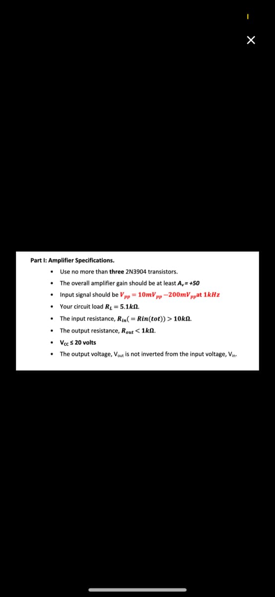
Transcribed Image Text:Part I: Amplifier Specifications.
• Use no more than three 2N3904 transistors.
• The overall amplifier gain should be at least A,= +50
• Input signal should be Vpp = 10mV pp -200mVppat 1kHz
• Your circuit load R, = 5.1kn.
• The input resistance, Rin( = Rin(tot)) > 10kn.
• The output resistance, Rout < 1kn.
• Vcc s 20 volts
• The output voltage, Vout is not inverted from the input voltage, Vin.
Expert Solution
This question has been solved!
Explore an expertly crafted, step-by-step solution for a thorough understanding of key concepts.

This is a popular solution!

Trending now
This is a popular solution!

Step by step
Solved in 6 steps with 2 images

Recommended textbooks for you
EBK ELECTRICAL WIRING RESIDENTIAL
Electrical Engineering
ISBN:
9781337516549
Author:
Simmons
Publisher:
CENGAGE LEARNING - CONSIGNMENT
EBK ELECTRICAL WIRING RESIDENTIAL
Electrical Engineering
ISBN:
9781337516549
Author:
Simmons
Publisher:
CENGAGE LEARNING - CONSIGNMENT