Q2\ The adder-subtractor circuit of Figure below has the following values for mode input M and data inputs X and Y. In each case, determine the values of the four SUM S outputs, the carry C, and overflow V. M a) 1 b) 0 X 01110 10110 FA Y 11010 10111 C₂ FA G S -* FA G FA C C₂ FA V V= V=
Q2\ The adder-subtractor circuit of Figure below has the following values for mode input M and data inputs X and Y. In each case, determine the values of the four SUM S outputs, the carry C, and overflow V. M a) 1 b) 0 X 01110 10110 FA Y 11010 10111 C₂ FA G S -* FA G FA C C₂ FA V V= V=

Electricity for Refrigeration, Heating, and Air Conditioning (MindTap Course List)
10th Edition
ISBN:9781337399128
Author:Russell E. Smith
Publisher:Russell E. Smith
Chapter17: Commercial And Industrial Air-conditioning Control Systems
Section: Chapter Questions
Problem 22RQ

Related questions
Question
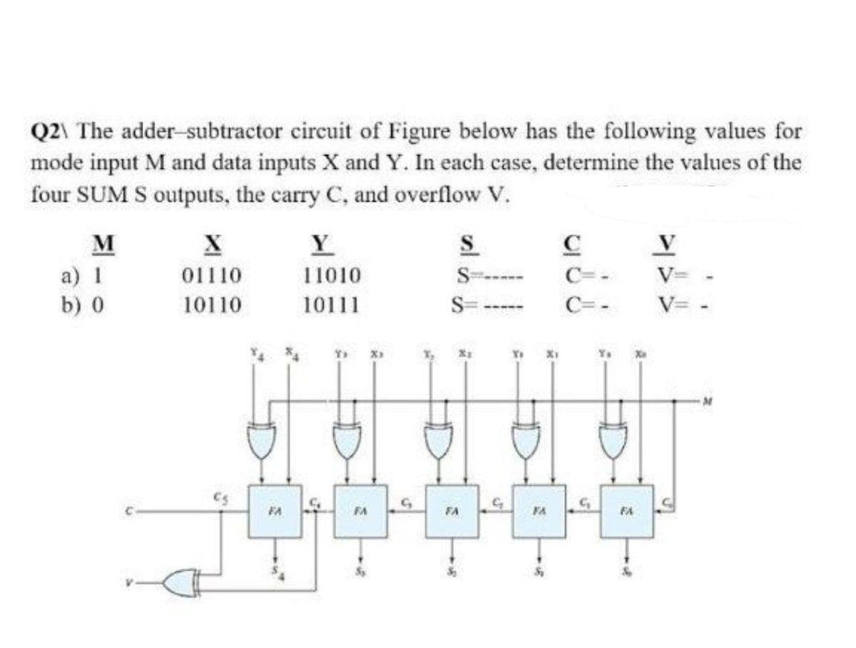
Transcribed Image Text:Q2\ The adder-subtractor circuit of Figure below has the following values for
mode input M and data inputs X and Y. In each case, determine the values of the
four SUM S outputs, the carry C, and overflow V.
M
a) 1
b) 0
X
01110
10110
Y
3
Y
11010
10111
FA
2
FA
S
7
G
FA
*
لون
C
C=
C₂
FA
V
V=
V=
Expert Solution
This question has been solved!
Explore an expertly crafted, step-by-step solution for a thorough understanding of key concepts.

Step by step
Solved in 5 steps with 5 images

Knowledge Booster


Learn more about
Need a deep-dive on the concept behind this application? Look no further. Learn more about this topic, electrical-engineering and related others by exploring similar questions and additional content below.Recommended textbooks for you
Electricity for Refrigeration, Heating, and Air C…
Mechanical Engineering
ISBN:
9781337399128
Author:
Russell E. Smith
Publisher:
Cengage Learning
Electricity for Refrigeration, Heating, and Air C…
Mechanical Engineering
ISBN:
9781337399128
Author:
Russell E. Smith
Publisher:
Cengage Learning