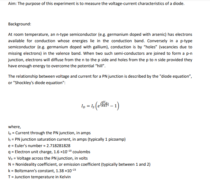
) The equation above contains really only three variables in it: Id, Vd, and T. All the other terms are constants. Since in most cases we assume temperature is fairly constant as well, we are really only dealing with two variables: diode current and diode voltage. Based on this realization, re-write the equation as proportionality rather than equality, showing how the two variables of diode current and voltage relate ii) Based on this simplified equation, what would an I vs V graph for a PN junction look like? How does this graph compare against the I vs V graph for a resistor? iii) When "P" and "N" type semiconductor pieces are brought into close contact, free electrons from the "N" piece will rush over to fill holes in the "P" piece, creating a zone on both sides of the contact region devoid of charge carriers. What is this zone called, and what are its electrical characteristics? iv) What happens to the thickness of the region in a PN junction (answer above) when an external voltage is applied to it? v) What effect will this change in this layer thickness, mentioned above, have on overall conductivity through the PN junction? Under what conditions will the conductivity be greatest, and under what conditions will the conductivity be least?


i) The equation above contains really only three variables in it: Id, Vd, and T. All the other terms are constants. Since in most cases we assume temperature is fairly constant as well, we are really only dealing with two variables: diode current and diode voltage. Based on this realization, re-write the equation as proportionality rather than equality, showing how the two variables of diode current and voltage relate
ii) Based on this simplified equation, what would an I vs V graph for a PN junction look like? How does this graph compare against the I vs V graph for a resistor?
iii) When "P" and "N" type semiconductor pieces are brought into close contact, free electrons from the "N" piece will rush over to fill holes in the "P" piece, creating a zone on both sides of the contact region devoid of charge carriers. What is this zone called, and what are its electrical characteristics?
iv) What happens to the thickness of the region in a PN junction (answer above) when an external voltage is applied to it?
v) What effect will this change in this layer thickness, mentioned above, have on overall conductivity through the PN junction? Under what conditions will the conductivity be greatest, and under what conditions will the conductivity be least?

Step by step
Solved in 2 steps with 2 images


