Q2. а. Draw the equivalent purely NOR gate representation of the function (Used bubble method). F (A,B,C,D) = (AB)(C+D) + A %3D b. From the waveform shown in figure 1, determine the following: I. Make truth table for output Q. II. Sketch the logic circuit that generate output Q by using NAND gate only.
Q2. а. Draw the equivalent purely NOR gate representation of the function (Used bubble method). F (A,B,C,D) = (AB)(C+D) + A %3D b. From the waveform shown in figure 1, determine the following: I. Make truth table for output Q. II. Sketch the logic circuit that generate output Q by using NAND gate only.

Chapter22: Sequence Control
Section: Chapter Questions
Problem 6SQ: Draw a symbol for a solid-state logic element AND.

Related questions

Question
100%
2- Please solve all of these questions with all steps. Thanks
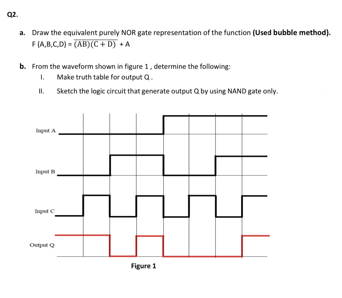
Transcribed Image Text:Q2.
а.
Draw the equivalent purely NOR gate representation of the function (Used bubble method).
F (A,B,C,D) = (AB)(C + D) + A
b. From the waveform shown in figure 1, determine the following:
Make truth table for output Q .
I.
I.
Sketch the logic circuit that generate output Q by using NAND gate only.
Input A
Input B
Input C
Output Q
Figure 1
Expert Solution
This question has been solved!
Explore an expertly crafted, step-by-step solution for a thorough understanding of key concepts.

Step by step
Solved in 7 steps with 10 images

Knowledge Booster


Learn more about
Need a deep-dive on the concept behind this application? Look no further. Learn more about this topic, electrical-engineering and related others by exploring similar questions and additional content below.Recommended textbooks for you