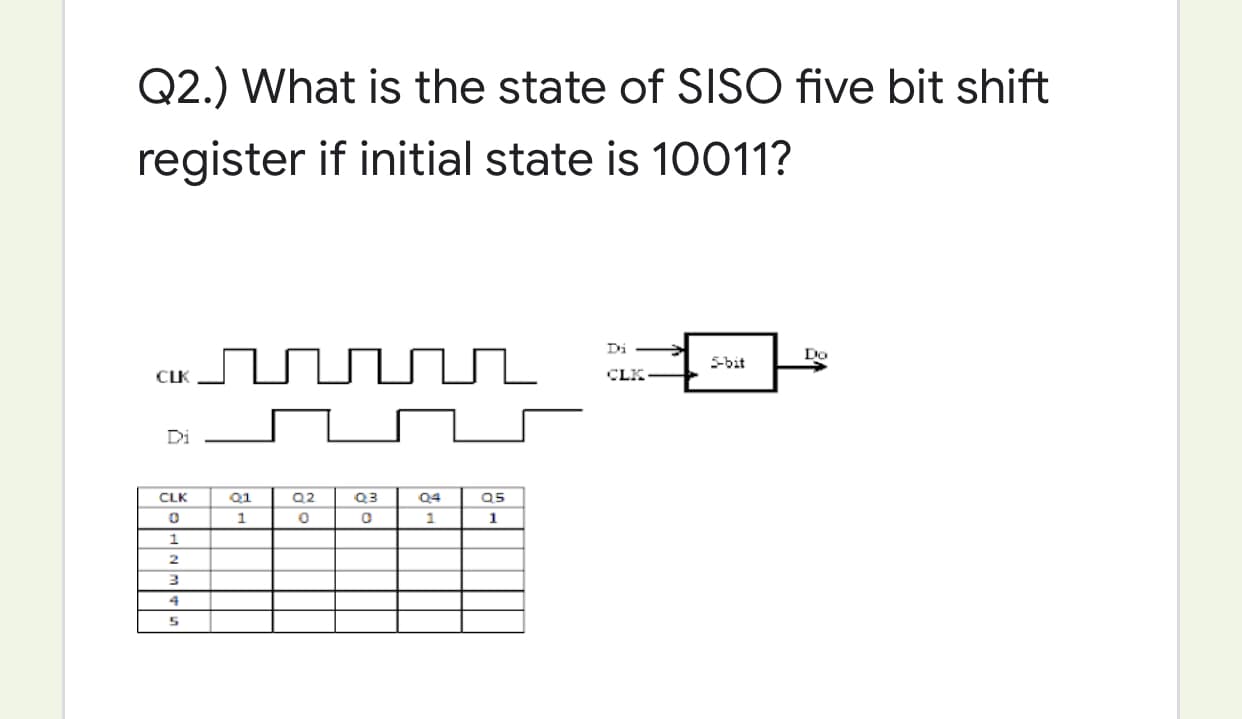
Q2.) What is the state of SISO five bit shift register if initial state is 10011? Di Do Sbit CLK CLK Di CLK Q1 Q2 Q3 Q4 Q5 1 1 4


Q: 1-Design a 4-bit ripple up counter using positive edge trigger J-K flip-flops.
A: As per our policy we can provide solution to first question only. 4-bit ripple up counter using…
Q: In the standard SOP expression, the binary words are formed by representing each non- complemented…
A: In the standard Sum of Products (SOP) expression, the binary words are formed by representing each…
Q: What is the hexadecimal value stored in Register A after the following assembler has executed? LDA…
A:
Q: a) Write VHDL code for an 8-bit shift register with data inputs and tri-state outputs. Use control…
A: Block diagram for an 8-bit register :
Q: 2. Let the data register AX have the content 67BF H. What would the PUSH AX command realize meaning…
A: AX =67BF H PUSH AX
Q: 20. Design a four-bit shift register with a parallel load, using D flip-flops. There are two control…
A: Four bit shift register with parallel load using D flip-flops is designed as shown below for the…
Q: write simple assignment statements vhdl code for 4 bit shift register using D Flip Flop
A:
Q: 32-Bit MIPS Register File Implement 32-Bit MIPS Register file (Zero Register...etc) CLK WE3 A1:…
A: Please find your answer below.
Q: Please design a cyclic shift right register with D flip flops
A: In cyclic shift register the shift out is fed back to the shift-in. It is basically the cascade…
Q: 1) Represent the numbers - (31), and – (17), in 6-bit signed-2's complement and perform -(31),0…
A:
Q: The 4-bit shift register shown was initially loaded with ABCD = 1000. List in the table below the…
A:
Q: 4- The following serial data are applied to the Flip - Flop below. Determine the resulting serial…
A:
Q: Q5/A- Indicate each of the following statement true or false and correct the false 1-Shift register…
A: As per our company guidelines we are supposed to answer only first 3 subpart kindly repost other…
Q: (b) Design 5-bit (Serial in/ Right /Parallel out) shift register.
A: LATCHES: Latches are a basic memory element that is used to store one bit of information. Types of…
Q: Consider a 4-bit shift register, with initial condition 1001, which is shifted right 5 times, while…
A:
Q: Q5/A- Indicate each of the following statement true or false and correct the false 1-Shift register…
A: We are authorized to answer three subparts at a time, since you have not mentioned which part you…
Q: Q 5. Determine the expression of the given logic circuit and simplify it. (using De'Morgan's law /…
A: NOR Gate NOR gate is a type of universal gate in which when all the inputs are low then the output…
Q: The number of inputs present in a logic gate denotes O a. Fan In O b. Fan Out О с Noise Margin O d.…
A: The number of input that a logic gate can handle is called Fan in.
Q: What bit mask will you need to isolate bit #6 for the AL register? (Give the hex number) Hint:…
A: 8 bit data of the AL register is b7 b6 b5 b4 b3 b2 b1 b0 our task is to isolate the #6 bit means b5…
Q: The group of bits 10011 is serially shifted into a 5-bit parallel output shift register with an…
A:
Q: Simplify the Boolean function F in sum of products using the don’t care condition: F (A, B, C) = Σ…
A: 3 variables has 8 possibilities. We have here 8 minterms including 3 don't cares Since don't cares…
Q: O2.) What ls the state of SISO five bit shift register if Initial otate le 10011? nnnnn
A:
Q: You have an 8-bit register A with initial value (10101010), . How can clear the least 2-bit, set the…
A: We are allowed to solve programming question only in assembly language, hence I have solved for the…
Q: Logical operations can be performed on strings of bits by considering each pair of corresponding…
A:
Q: 1. How a 5 bit Asynchronous decade counter can be implemented having a modules of ten with a…
A: "According to the company's policy we will provide solution of the first question since the other…
Q: 1) Represent the numbers - (31)10 and - (17)1, in 6-bit signed-2's complement and perform -(31),0…
A:
Q: a) For a two-input OR gate, Find the standard SOP and POS expressions as a function of input…
A:
Q: The number of inputs present in a logic gate denotes O a. Fan In O b. Noise Margin O c. Propgation…
A: Fan in : the number of inputs that can be connected to a circuit. Noise margin: is the ratio by…
Q: In the standard SOP expression, the binary words are formed by representing each complemented…
A: The boolean algebra involves various boolean operations like NOT, AND and OR. The boolean algebra…
Q: Q2) a) design 4-bit register with parallel load b) design 4-bit Serial In/Serial Out Shift Registers
A: 2) a) 4-bit register with parallel load Parallel-load registers are a sort of register where the…
Q: O Find the output PN sequence of the following shift register. The initial state of the register is…
A: Since you have asked multiple questions, we will solve the first question for you. If you want any…
Q: Design a 4-bit Register Using D Flip Flops and MUXs with the following mode of operation: 00:…
A: this can be implement with help of universal register. Truth table is shown below S1 S0…
Q: 1. Construct a table all possible m=4 bit sequences. Assuming 1 bit is used for representing the…
A: According to the question, we need to construct a table for m=4 bit sequence. Assuming 1 bit is used…
Q: Q4. Draw the logic circuits for the given Boolean Functions: - 1. F=XꚚYꚚZ Z= xy+yz+zx 2.…
A:
Q: Procedure: 1. Design an even/odd parity generator for 4-bit data. 2. Design a parity checker circuit…
A: As per policy attempting first question For 4 bit data even parity generator
Q: Q2) a) design 4-bit register with parallel load b) design 4-bit Serial In Serial Out Shift Registers
A:
Q: a) An 8-bit shift register holds the data word 00111100. What will the register contents be after…
A: From the right shift register..
Q: The 4-bit shift register shown was initially loaded with ABCD = 0110 . List in the table below the…
A: We should determined register contents A,B,C,D After clock pulse 1 & 2
Q: draw the logic diagram for F=YZ’ + X’Y’Z
A:
Q: 1) Find the bitwise operations ⨁ of each pair of bit strings: 1011 0000 , 0100 1010.
A: We are authorized to answer one question at a time, since you have not mentioned which question you…
Q: Create a 5-bit shift right register using D flip-flops. Given an initial value of Din=1 and Q4 Q3 Q2…
A:
Q: In the logic circuit given below, determine the bit sequence at the output of the data-selector…
A: The initial values of each register when the clock is not applied.
Q: The state of a 12-bit register is 100010010111. What is its content if it represents Three decimal…
A: BCD equivalent of the given binary number can be obtained by dividing the given binary number into 4…
Q: Q4. Draw the logic diagram of a four-bit register with four D flip-flops and four 4x1 multiplexers…
A: Refer provided table in the question The circuit consists of four D flip flops and four…
Q: Simplify the Boolean function and design its logic gate C(x, y, z) =…
A: K-Map is used to solve a boolean function in optimized way and to make the truth table using the…
Q: The contents of a four bit register are initially 1011.The register is shifted six times to the…
A: Shift register is used to store multiple bits of data using group of flip flops. By using the clock…
Q: How many shift pulses are needed to serially shift the contents of a 3 bit register to another 3 bit…
A: As per our company guidelines we are supposed to answer only first question kindly repost other…
Q: How many full adder circuits are needed to add five bit binary numbers. O a. 5 O b. 7 O c. 10 O d. 2
A: In this question , we will write about how many full adder are required to add 2 five bit binary…
Q: Q5/A- Indicate each of the following statement true or false and correct the false 1-Shift register…
A: As per honour code , for multiple questions we are advised to answer first question only. please…

Step by step
Solved in 3 steps with 3 images


- A 12-bit D/A converter has VREF = 5.12 V. What is the output voltage for a binary input code of (101010101010)? What is VLSB? What is the size of the MSB?Subject Digital Logic Design(DLD) Design the truth table for Full Subtractor Circuit. Write the Boolean expression for Difference andBorrow. Also Draw the circuit diagram for Difference and Borrow.Q1) Design a counter that has clk and rst as input and 4 bit output. The counter counts in the following sequence: 2-5-8-11-14-1-4-7-10-13-0-3-6-9-12-15
- Give the logic diagram of half subtractor. NOTE: SUB: DIGITAL LOGIC AND DESIGN(DLD) DEPTT:CS/IT.Adders are digital circuits in electronics that implement addition of binary numbers. Given two numbers A= 01111100 and B = 01011010, use the concept of ripple carry adders to find A+B. Using an illustration, explain in detail how the full adders are joined together to carry out the addition of these 8-bit numbers.(DIGITAL LOGIC DESIGN QUESTION) Q2. Take the number N created from your actual registration number (EF20BCE013 above, anda) convert it into binaryb) encode it into binary using BCD code.
- Generate a parameterized and portable Verilog model of an 8-bit ring counter whose movement is from its MSB(Most significant Bit) to its LSB(Leat Significant Bit).Design a circuit called half adder (HA) which adds two 1-bit numbers, a,b and produces 2-bit output, c. a. Draw the truth table of the circuit.b. Find the Boolean functions of each bit of the output.c. Optimize the Boolean functions.d. Draw the logic diagram of the optimized circuits.e. Write the VHDL code of the logic diagrams by using “Dataflow modeling” method f. Simulate the circuits that you have designed in 1.e. Prepare a simulation waveform for you report.g. Produce the RTL schematic for the circuit that you have designed in 1.e.Design an Implementation of 8-bit Floating Light Digital Circuit Implementation Using D Flip-Flop. Interpret the results. (Hint: Using Shift Register)
- Give the internal logic for the 2-to-1 multiplexer on 4-bit data paths by giving the four outputs each as a logic expression of the nine inputs.1:The output of a logic gate is 1 when all the input are at logic 1 and a . OR and EX - NOR Gate b . AND Gate and EX - OR Gate C. OR and EX - OR Gate d . NAND and OR Gate 2: Choose an application of A / D convertor a. Sonar systems b. Radars and Jammers C. Digital Audio apllications d. Encoders 3: Find the simplification of AB + B ( B + C ) + C ( B + C ) a. C + A b. B + C c. 1 d. A + 4: Choose a correct number of input lines for a decoder which has 128 output lines a . 14 b . 7 c . 1 d . 128 6: Select a suitable example for sequential logic circuit . a . Encoder b . None of the given choices c . Counters d . PALNAND gates require one less transistor thanAND gates. They are often used exclusively toconstruct logic circuits. One such logic circuit that usesthree-input NAND gates is shown in Figure P12.25.a. Determine the truth table for this circuit.b. Give the logic equation that represents the circuit(you do not need to reduce it).