th cases, the coolant is a dielectric liquid at 20°C. A heat transfer c of the unfinned package and on all surfaces of the exposed silicon nk includes a 50 x 50 array of nanofins. Determine the maximum a that its temperature is maintained at T, < 75°C for (a) the unfinn
th cases, the coolant is a dielectric liquid at 20°C. A heat transfer c of the unfinned package and on all surfaces of the exposed silicon nk includes a 50 x 50 array of nanofins. Determine the maximum a that its temperature is maintained at T, < 75°C for (a) the unfinn
Principles of Heat Transfer (Activate Learning with these NEW titles from Engineering!)
8th Edition
ISBN:9781305387102
Author:Kreith, Frank; Manglik, Raj M.
Publisher:Kreith, Frank; Manglik, Raj M.
Chapter2: Steady Heat Conduction
Section: Chapter Questions
Problem 2.17P

Related questions

Question
silicon carbide (T ≈ 300 K): k = 490 W/m⋅K
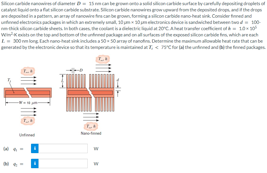
Transcribed Image Text:Silicon carbide nanowires of diameter D = 15 nm can be grown onto a solid silicon carbide surface by carefully depositing droplets of
catalyst liquid onto a flat silicon carbide substrate. Silicon carbide nanowires grow upward from the deposited drops, and if the drops
are deposited in a pattern, an array of nanowire fins can be grown, forming a silicon carbide nano-heat sink. Consider finned and
unfinned electronics packages in which an extremely small, 10 µm x 10 μm electronics device is sandwiched between two d = 100-
nm-thick silicon carbide sheets. In both cases, the coolant is a dielectric liquid at 20°C. A heat transfer coefficient of h = 1.0×10⁵
W/m².K exists on the top and bottom of the unfinned package and on all surfaces of the exposed silicon carbide fins, which are each
L = 300 nm long. Each nano-heat sink includes a 50 × 50 array of nanofins. Determine the maximum allowable heat rate that can be
generated by the electronic device so that its temperature is maintained at T, < 75°C for (a) the unfinned and (b) the finned packages.
T., h
-W= 10 μm-
T., h
Th
Unfinned
(a) 9₁ =
(b) 9₂ =
i
i
D
Th
Nano-finned
W
W
T
Expert Solution
This question has been solved!
Explore an expertly crafted, step-by-step solution for a thorough understanding of key concepts.

Step by step
Solved in 4 steps with 19 images

Knowledge Booster


Learn more about
Need a deep-dive on the concept behind this application? Look no further. Learn more about this topic, mechanical-engineering and related others by exploring similar questions and additional content below.Recommended textbooks for you
Principles of Heat Transfer (Activate Learning wi…
Mechanical Engineering
ISBN:
9781305387102
Author:
Kreith, Frank; Manglik, Raj M.
Publisher:
Cengage Learning
Principles of Heat Transfer (Activate Learning wi…
Mechanical Engineering
ISBN:
9781305387102
Author:
Kreith, Frank; Manglik, Raj M.
Publisher:
Cengage Learning