The linear electron and hole concentration profiles in a 4 um wide region of silicon material is shown in the figure below. The silicon material is subjected to electron injection from the left and hole injection from the right as shown in the figure. Assume that the cross-sectional area of the material A = 1 um?, electron mobility Hn = 1312.75 cm² /V s, and hole mobility Hp = 463.33 cm2 /V s. Find the total current (to one decimal place) flowing through the material. T = 300K, q = 1.6 x 10⁻¹⁹ C, k = 8.62 x 10⁻⁵ eV/K, k = 1.38 x 10⁻²³ J/K, and 1 eV = 1.6 x 10⁻¹⁹ C. 6 x 10¹⁷/cm3 3 x 10¹⁷/cm3 Electrons Holes x = 0 x = 4 µm
The linear electron and hole concentration profiles in a 4 um wide region of silicon material is shown in the figure below. The silicon material is subjected to electron injection from the left and hole injection from the right as shown in the figure. Assume that the cross-sectional area of the material A = 1 um?, electron mobility Hn = 1312.75 cm² /V s, and hole mobility Hp = 463.33 cm2 /V s. Find the total current (to one decimal place) flowing through the material. T = 300K, q = 1.6 x 10⁻¹⁹ C, k = 8.62 x 10⁻⁵ eV/K, k = 1.38 x 10⁻²³ J/K, and 1 eV = 1.6 x 10⁻¹⁹ C. 6 x 10¹⁷/cm3 3 x 10¹⁷/cm3 Electrons Holes x = 0 x = 4 µm

Power System Analysis and Design (MindTap Course List)
6th Edition
ISBN:9781305632134
Author:J. Duncan Glover, Thomas Overbye, Mulukutla S. Sarma
Publisher:J. Duncan Glover, Thomas Overbye, Mulukutla S. Sarma
Chapter4: Transmission Line Parameters
Section: Chapter Questions
Problem 4.2P: The temperature dependence of resistance is also quantified by the relation R2=R1[ 1+(T2T1) ] where...

Related questions

Question
The linear electron and hole concentration profiles in a 4 um wide region of silicon material is shown in the figure below. The silicon material is subjected to electron injection from the left and hole injection from the right as shown in the figure. Assume that the cross-sectional area of the material ?=1 ??2, electron mobility ??=1312.75 ??2/? ?, and hole mobility ??=463.33 ??2/? ?. Find the total current (to one decimal place) flowing through the material.
?=300?, ?=1.6×10⁻¹⁹ ?, ?=8.62×10⁻⁵ ??/?, ?=1.38×10⁻²³ ?/?, and 1 ??=1.6×10⁻¹⁹ ?.
Explain how depletion and diffusion capacitances differ
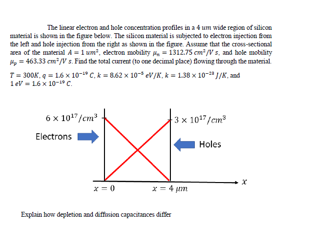
Transcribed Image Text:The linear electron and hole concentration profiles in a 4 um wide region of silicon
material is shown in the figure below. The silicon material is subjected to electron injection from
the left and hole injection from the right as shown in the figure. Assume that the cross-sectional
area of the material A = 1 um?, electron mobility Hn = 1312.75 cm² /V s, and hole mobility
H, = 463.33 cm?/V s. Find the total curent (to one decimal place) flowing through the material.
T = 300K, q = 1.6 x 10⁻¹⁹ C, k = 8.62 x 10⁻⁵ eV/K, k = 1.38 x 10⁻²³ J/K, and
1eV %3D 1.6 х 10-19 С.
6 x 10¹⁷/cm3
3 x 10¹⁷/cm3
Electrons
Holes
x = 0
x = 4 µm
Explain how depletion and diffusion capacitances differ
Expert Solution
This question has been solved!
Explore an expertly crafted, step-by-step solution for a thorough understanding of key concepts.

This is a popular solution!

Trending now
This is a popular solution!

Step by step
Solved in 2 steps with 2 images

Knowledge Booster


Learn more about
Need a deep-dive on the concept behind this application? Look no further. Learn more about this topic, electrical-engineering and related others by exploring similar questions and additional content below.Recommended textbooks for you
Power System Analysis and Design (MindTap Course …
Electrical Engineering
ISBN:
9781305632134
Author:
J. Duncan Glover, Thomas Overbye, Mulukutla S. Sarma
Publisher:
Cengage Learning
Power System Analysis and Design (MindTap Course …
Electrical Engineering
ISBN:
9781305632134
Author:
J. Duncan Glover, Thomas Overbye, Mulukutla S. Sarma
Publisher:
Cengage Learning