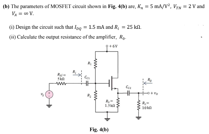
The parameters of MOSFET circuit


Q: Please create a truth table for the below transistor diagram and explain. Thank you! 1 a b output
A:
Q: Explain three reasons why MOSFETs are typically used in computers instead of BJTs.
A: Reason for using MOSFETs instead of BJTs in computers are = (1) Physical size of MOSFET is less than…
Q: Common-gate MOSFET:
A:
Q: 3) Draw the Input and output Characteristics of BJT for CE configuration
A: The above question is related to the topic of Electronics Devices And Circuits Input output…
Q: MOSFET can act as a switch in active region. Select one: True False
A: The explanation is as follows.
Q: 3. Write any three differences between FET and MOSFET
A: The differences between the FET and the MOSFET are listed in the tables shown below: FET MOSFET…
Q: Compare a BJT with a MOSFET regarding their transconductances and current efficiencies.
A:
Q: For npn transistor in the active mode, the base voltage is the emitter voltage greater than less…
A:
Q: List three conditions need to be considered to choose a MOSFET for switching applications.
A: Following are the most important conditions to be considered when choosing a MOSFET for switching…
Q: Explain the relationship between Ip and Vps of MOSFET.
A: The relationship between ID and VDS of MOSFET is called output transfer characteristics.
Q: Power MOSFET Operating modes
A: MOSFET is a semiconductor device used for the purpose of switching and amplifying electronic…
Q: PROBLEM 7.15 Determine VOUT versus vIN for the circuit shown in Figure 7.8 Assume that the MOSFET…
A: We are authorized to answer one question at a time, since you have not mentioned which question you…
Q: The parameter which acts as a control for switching a MOSFET is
A: The MOSFET (Metal Oxide Semiconductor Field Effect Transistor) transistor is a semiconductor device…
Q: When an n-channel D-MOSFET has Ip > Ipss, it O Is operating in the enhancement mode Is forward…
A: In this question we need to choose a correct option
Q: 2. The MOSFET in the following circuit is in which configuration?
A: The solution is provided in the following section.
Q: How do you determine when a transistor is in cutoff? A when Væ = 0V (B) when VCE = Vcc when VCE =…
A:
Q: 3. Fo the fix bias configuration below, determine the Ipo, VDSQ and VD
A:
Q: Discuss and analyze the biasing methods of E-MOSFET and D-MOSFET.
A:
Q: Give the circuit of level transitor? (Draw Emitter follower with voltage divider)
A: Amplifier is an electronic device whose output is amplified version of the input signal. The…
Q: The dc voltages at the bases and emitters of the tr
A:
Q: 1. Compare JFET and MOSFET transistors in terms of its characteristics, functionality and…
A: JFET : Junction field effect transistor MOSFET: Metal-oxide-semiconductor field effect transistor.…
Q: True and false (if false what is the correct with the reason) 5- Unlike JFETs and D-MOSFETs, the…
A: According to question we have to discuss Unlike JFETs and D-MOSFETs, the E-MOSFET cannot operate…
Q: IGBT is a short form of Insulated Gate Bipolar Transistor, combination of Bipolar Junction…
A: The comparison table on above characteristic is given below
Q: State the advantage of using transistors in place of resistors in MOSFET inte- grated circuits.
A: The transistors in the integrated circuits are used for replacing the resistor, the reason behind…
Q: Draw the symbol of enhancement and depletion N channel MOSFET.
A:
Q: Differentiate E-MOSFET and DE –MOSFET
A: Differentiate E-MOSFET and DE –MOSFET.
Q: 4 The voltage that turns on an E-MOSFET device is the.. ...voltage. 5 The transfer characteristic…
A: Solution 4. Threshold. The voltage that turns on an E-MOSFET device is the threshold voltage.
Q: compares as points and try to make the answer short b) Explain the main differences between BJT…
A: In this question, we have to differentiate between BJT, MOSFET and IGBT..
Q: Calculate the threshold voltage of an n-channel MOSFET
A:
Q: -Write short notes on the following : (i) Advantages of JFET Difference between MOSFET and JFET (ii)
A: JFET-JFET stand for junction field effect transistor.It is like as normal FET. The types of JFET…
Q: Explain the use of Metal Oxide Varistors MOVs
A: MOVs (Metal oxide varistors) is a variable resistor whose resistance is changed with respect to…
Q: 4. Sketch the drain characteristics of the JFET from the obtained data.
A: Since you have asked multiple questions, we will solve the first question for you. If you want any…
Q: An emitter follower configuration has the following bigs:
A: NOTE- “Since you have posted a question with multiple sub-parts, we will solve first three subparts…
Q: 3) Draw the Input and output Characteristics of BJT for CB configuration
A:
Q: circuit components. A three-input CML XOR gate using BJTS (bipolar junction transistors) is shown…
A: In this question we will write about list of electrical circuit components....
Q: b) Design a MOSFET NOR circuit
A: MOSFET: Metal-oxide-semiconductor field-effect transistor (MOSFET) is an acronym for a…
Q: Explain the turn on of SCR based on two transistor model?
A: Two transistor model of Thyristor- The basic operation of the thyristor can easily find out by two…
Q: Discuss the significant different between the construction of an E-MOSFET and a D-MOSFET.
A: Question- Discuss the significant different between the construction of an E-…
Q: Which of the following is true about the D-type MOSFETS?
A: In the depletion MOSFET (D-MOSFET), the conducting channel is already present between the source and…
Q: Draw the equivalent circuit model and switching characteristics of the device which is used for low…
A: MOSFET is a device which is used for low on state loss and high switching frequency operation.…
Q: • What type of MOSFET whose channel is originally thick but narrows as the proper gate bias is…
A: MOSFET stands for metal oxide semiconductor field effect transistor. MOSFET is a voltage controlled…
Q: For the Depletion-type MOSFET n
A:
Q: 9.2 / what are the majority carriers in base region of an nfn transistor callel ?
A: Before getting in to the actual question lets get in to some basics Electrical symbol of NPN…
Q: (BJT Amplifiers)
A:
Q: Determine the working point of the transistor shown in the next circuit
A:
Q: What are the advantages of MOSFET over JFET?
A: MOSFET are used in various applications due to its simple working phenomena and advantages over…

Step by step
Solved in 3 steps with 3 images


- In the common-emitter amplifier circuit shown in the figure, Vcc=9V, R1=27kΩ, R2=15kΩ, RE=1.2kΩ and RC=2.2kΩ. The transistor has β=100.a-) If Rsig=10kΩ and RL=2kΩ, calculate the IE value of the amplifier.b-) For small signal analysis of the transistor, find the value of Rin by deriving the π-modelc-) Calculate vo/vsig and io/ii.Design a Single-Stage Common Emitter Class A Amplifier Specifications:Voltage Divider Bias Circuit Supply: Any value from 10Vdc to 24VdcLoad: 1kΩVoltage Gain: Any value from 80 to 400Lower Cutoff Frequency: 100 HzSinusoidal source (zero internal resistance): 50mVp-pTransistor: Si, β = 75 • Base-Collector capacitance = 8pF • Base-Emitter Capacitance = 25pF a) compute for the biasing resistances.b) determine the dc transistor terminal voltages and transistor currents.(a) What are the Q-points for the transistors in the amplifier as shown if VCC = 15 V, VEE = 15 V, IEE = 400 μA, βF = 100, REE = 270 kΩ,RC =47 kΩ, VA=∞, and βF =100? (b) What are the differential-mode gain, common-mode gain, CMRR, and differential-mode and common-modeinput and output resistances? (c) Repeat part (b) for VA = 50 V.
- (a) What are the Q-points for the transistors in the amplifier as shown if VDD =5V, VSS =5 V, RSS =2.4 kΩ, and RD =2.4 kΩ? Assume Kn =400 μA/V2 and VT N =0.7 V. (b) What are the differential-mode gain, common-mode gain, CMRR, and differential-mode and common-mode input resistances?The dc bias circuit for a common emitter amplifier is shown in the figure. In the circuit, Vcc=15v,RB1=20k Ω,RB2=100k Ω,Rc=5.1k Ω,and RE1=1k Ω, Assume that when the transistor is on, the voltage drop from base to emitter VBE=0.7v. Also assume that β= ∞, which implies that the base current can be considered zero (IB=0) in your calculations. Solve for the base voltage VB. Solve for the emitter voltage VE. Solve for the emitter current IB. Solve for the collector current ICConsider the common-source amplifier shown in Figure P11.50. The NMOS transistor has KP=50 μA/V2, L=5 μm, W=500 μm, Vto=1 V and rd=∞.a. Determine the values of IDQ, VDSQ and gm. b. Compute the voltage gain, input resistance, and output resistance, assuming that the coupling capacitors are short circuits for the ac signal. Repeat Problem P11.50 for an NMOS transistor having KP=50 μA/V2, W=600 μm, L=20 μm, Vto=2 V and rd=∞. Compare the gain with that attained in Problem P11.50.
- Vs=100 mV peak-to-peak, 1 kHz sine signal, Kn=0.4mA/v^2 ,Vt=1V , λ=0.01V^-1 Make the DC analysis of the above given mosfet amplifier circuit. Simulation to tableWrite down the measured values and mathematical calculation results. (The valueswith the units.)DC Parameters ,Measured value ,Calculated ValueVGETCVGSVDVDSIDb. Draw the small signal model for the AC analysis of the circuit. Find the gm, ro, Av values.c. Show the Vs input signal and the Vo output signal of the circuit on the oscilloscope. Volt/div of channels andSpecify time/div values.The common-emitter amplifier given in the figure in the circuit, Vcc=9V, R1=27kΩ, R2=15kΩ, RE=1.2kΩ and RC=2.2kΩ. Transistor β=100 has value. a-) If it has values of Rsig=10kΩ and RL=2kΩ Calculate the IE of the amplifier. b-) For small signal analysis of transistor Find the value of Rin by deriving the π-model c-) Calculate vo/vsig and io/ii.(a) What are the Q-points for the transistors in the amplifier as shown if VDD = 12V, VSS = 12V, ISS = 1.5 mA, RSS = 33 kΩ, and RD = 15 kΩ? Assume Kn = 375 μA/V2 and VT N = 0.75 V. (b) What are the differential-mode gain, commonmode gain, CMRR, and differential-mode and common-mode input resistances?
- 4) By drawing the small signal model of the circuit given below, we can determine the total voltage and current gain values of the circuit, without the bypass capacitor on and without the bypass capacitor. Calculate separately for the two cases as it will be in the circuit (connected to the emitter end of the transistor). (β = 100, rS = 600 Ω, R1 = 27 KΩ, R2 = 4.7 KΩ, RC = 3.3 KΩ, RE = 680 Ω, RL= 15 KΩ, VCC = 10 V)(a) What are the Q-points for the transistors in the amplifier as shown if VDD = 9 V, VSS = 9 V, ISS = 40 μA, RSS = 1.25 MΩ, and RD = 300 kΩ? Assume Kp = 200 μA/V2, γ = 0.6 V0.5, 2φF = 0.6 V, and VTO = −1 V. (b) What are the differential-mode gain, common-mode gain, CMRR, and differential-mode and common-mode input resistances?For the amplifier as shown, VDD = 12 V, VSS = 12 V, ISS = 20 μA, and RD = 820 kΩ. Assume IDSS = 1 mA and VP = +2 V. (a) What are the output voltages υo for the amplifier for υ1 = 0V and υ1 = 20 mV? (b) What is the maximum permissible value of υs?