Therefore, (a) In a multi-bit add operation, the input carry Cin is we introduce three carry status generate (G), to describe the carry status. Please writ P, and G using the three inputs: A, B, and Cin.
Therefore, (a) In a multi-bit add operation, the input carry Cin is we introduce three carry status generate (G), to describe the carry status. Please writ P, and G using the three inputs: A, B, and Cin.

Chapter22: Sequence Control
Section: Chapter Questions
Problem 6SQ: Draw a symbol for a solid-state logic element AND.

Related questions
Question
Please do not rely too much on chatgpt, because its answer may be wrong. Please consider it carefully and give your own answer. You can borrow ideas from gpt, but please do not believe its answer.Very very grateful!Please do not rely too much on chatgpt, because its answer may be wrong. Please consider it carefully and give your own answer. You can borrow ideas from gpt, but please do not believe its answer.Very very grateful!
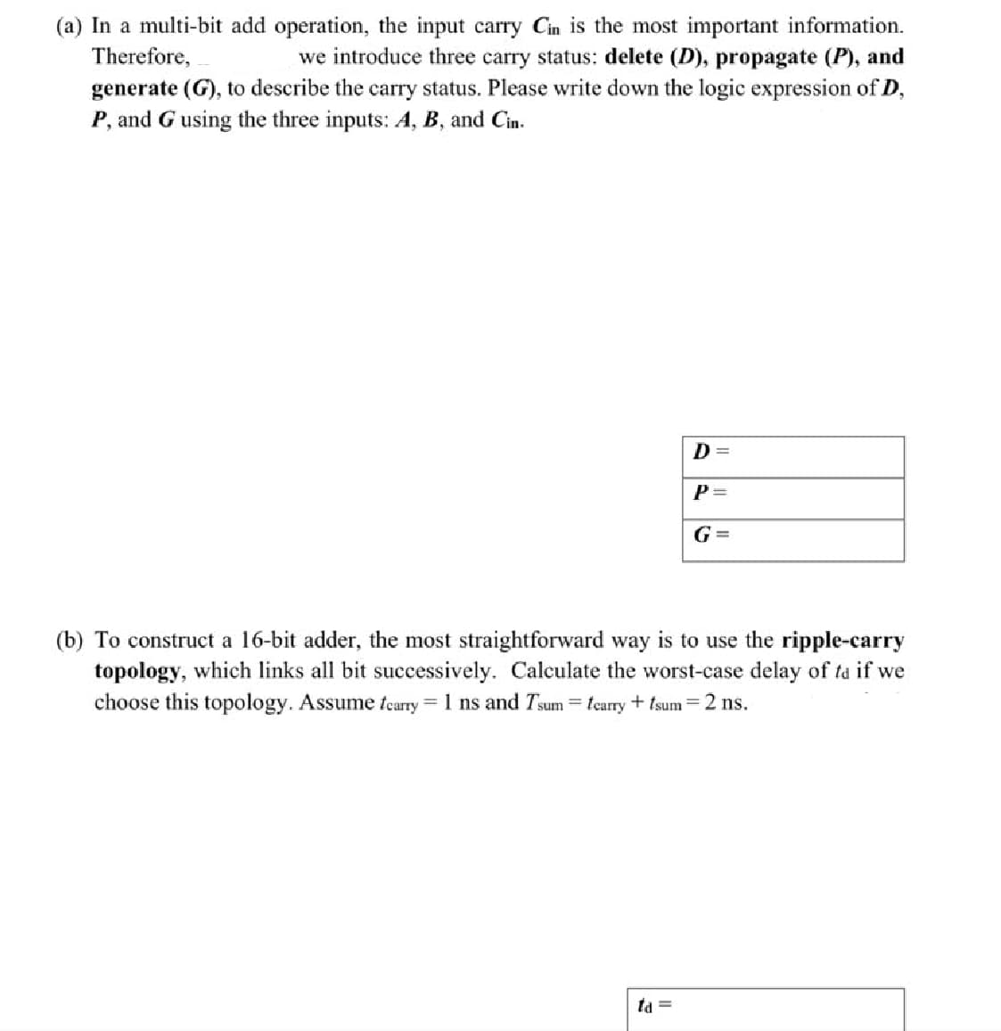
Transcribed Image Text:(a) In a multi-bit add operation, the input carry Cin is the most important information.
Therefore,
we introduce three carry status: delete (D), propagate (P), and
generate (G), to describe the carry status. Please write down the logic expression of D,
P, and G using the three inputs: A, B, and Cin.
D =
td =
P=
G=
(b) To construct a 16-bit adder, the most straightforward way is to use the ripple-carry
topology, which links all bit successively. Calculate the worst-case delay of ta if we
choose this topology. Assume fearry = 1 ns and Tsum = tcarry + tsum=2 ns.
Expert Solution
This question has been solved!
Explore an expertly crafted, step-by-step solution for a thorough understanding of key concepts.

Step by step
Solved in 3 steps with 10 images

Knowledge Booster


Learn more about
Need a deep-dive on the concept behind this application? Look no further. Learn more about this topic, electrical-engineering and related others by exploring similar questions and additional content below.Recommended textbooks for you