This is a three-part question about critical path calculation. Consider a simple single-cycle implementation of LEGv8 ISA. The operation times for the major functional components for this machine are as follows: Component Latency ALU 90 ps Add 70 ps ALU Control Unit 30 ps Shifter 20 ps Control Unit/ROM 50 ps Sign/zero extender 20 ps 2-1 MUX 20 ps Memory (read/write) (instruction or data) 140 ps PC Register (read action) 20 ps PC Register (write action) 20 ps Register file (read action) 80 ps Register file (write action) 60 ps Logic (1 or more levels of gates) 10 ps Below is a copy of the LEGv8 single-cycle data path design. In this implementation the clock cycle is determined by the longest possible path in the machine. The critical paths for the different instruction types that need to be considered are: R-format, Load-word, and store-word.


How can I compute sum of each of the component latencies for each instruction?
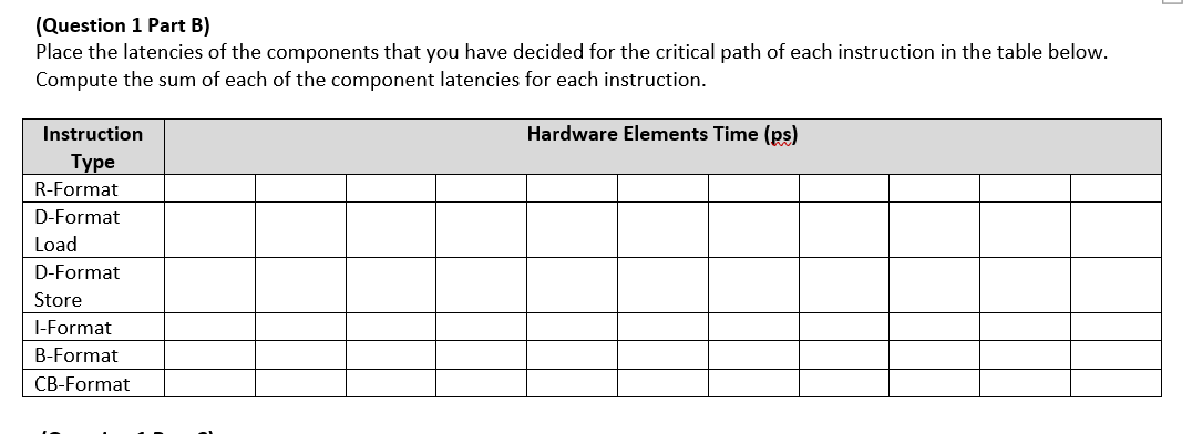
Question 1:
This is a three-part question about critical path calculation. Consider a simple single-cycle implementation of LEGv8 ISA. The operation times for the major functional components for this machine are as follows:
Component Latency
|
ALU |
90 ps |
|
Add |
70 ps |
|
ALU Control Unit |
30 ps |
|
Shifter |
20 ps |
|
Control Unit/ROM |
50 ps |
|
Sign/zero extender |
20 ps |
|
2-1 MUX |
20 ps |
|
Memory (read/write) (instruction or data) |
140 ps |
|
PC Register (read action) |
20 ps |
|
PC Register (write action) |
20 ps |
|
Register file (read action) |
80 ps |
|
Register file (write action) |
60 ps |
|
Logic (1 or more levels of gates) |
10 ps |
Below is a copy of the LEGv8 single-cycle data path design. In this implementation the clock cycle is determined by the longest possible path in the machine. The critical paths for the different instruction types that need to be considered are: R-format, Load-word, and store-word.
![Below is a copy of the LEGV8 single-cycle data path design. In this implementation the clock cycle is determined by the
longest possible path in the machine. The critical paths for the different instruction types that need to be considered are:
R-format, Load-word, and store-word.
PC
Read
address
Add
Instruction
memory
Instruction
[31-0]
Instruction [31-26]
Instruction [25-21]
Instruction [20-16]
Instruction [15-11]
Instruction [15-0]
Control
1
RegDst
Branch
MemRead
MemtoReg
ALU Op
MemWrite
ALU Src
RegWrite
Read
register 1
Read
register 2
Write
register
Write
data
Registers Read
data 2
16
Read
data 1
Instruction [5-0]
Sign
extend
32
Shift
left 2
OMUX-
ALU
control
Add
ALU
result
Zero
>ALU ALU
result
1
Address
Write
data
PCSrc
Read
data
Data
memory
OXER](/v2/_next/image?url=https%3A%2F%2Fcontent.bartleby.com%2Fqna-images%2Fquestion%2F8118e386-612e-473a-ac24-98651a38be26%2F84f9a5d8-fe32-4703-97f1-b5308dff8789%2F65atspo_processed.png&w=3840&q=75)


Trending now
This is a popular solution!

Step by step
Solved in 4 steps


