truth table, then simplify that expression as much as possible, and draw a logic gate circuit equivalent to that simplified expression: * ABC Output 00 0 1 00 1 1 01 0 011 1 10 0 10 1 1 11 0 1 111 1
truth table, then simplify that expression as much as possible, and draw a logic gate circuit equivalent to that simplified expression: * ABC Output 00 0 1 00 1 1 01 0 011 1 10 0 10 1 1 11 0 1 111 1

Chapter22: Sequence Control
Section: Chapter Questions
Problem 6SQ: Draw a symbol for a solid-state logic element AND.

Related questions
Question
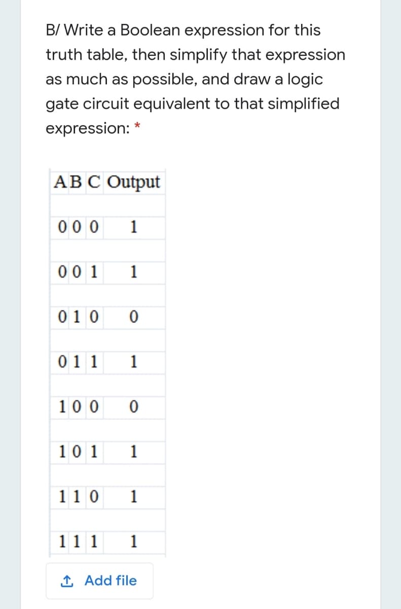
Transcribed Image Text:B/ Write a Boolean expression for this
truth table, then simplify that expression
as much as possible, and draw a logic
gate circuit equivalent to that simplified
expression: *
АВС Output
00 0
1
00 1
1
010
011
1
100
10 1
1
11 0
1
11 1
1
1 Add file
Expert Solution
This question has been solved!
Explore an expertly crafted, step-by-step solution for a thorough understanding of key concepts.

This is a popular solution!

Trending now
This is a popular solution!

Step by step
Solved in 2 steps with 1 images

Knowledge Booster


Learn more about
Need a deep-dive on the concept behind this application? Look no further. Learn more about this topic, electrical-engineering and related others by exploring similar questions and additional content below.Recommended textbooks for you