Using Table P.1, For the following figure 4 if R1 = 1000 and VIN = 1V answer the following questions: +Vcc VIN 6. VOUT Vee ww. R2 R1 GND Fig. p.4 a) What is the fig.4 circuit name? b) In fig.7 if R2 = 4000, determine the Gain K? Show all steps c) In fig.7 if R2 = 4000, determine the VOUT? Show all steps d) In fig.7 if VOUT = 6V, determine the R2? Show all steps
Using Table P.1, For the following figure 4 if R1 = 1000 and VIN = 1V answer the following questions: +Vcc VIN 6. VOUT Vee ww. R2 R1 GND Fig. p.4 a) What is the fig.4 circuit name? b) In fig.7 if R2 = 4000, determine the Gain K? Show all steps c) In fig.7 if R2 = 4000, determine the VOUT? Show all steps d) In fig.7 if VOUT = 6V, determine the R2? Show all steps

Introductory Circuit Analysis (13th Edition)
13th Edition
ISBN:9780133923605
Author:Robert L. Boylestad
Publisher:Robert L. Boylestad
Chapter1: Introduction
Section: Chapter Questions
Problem 1P: Visit your local library (at school or home) and describe the extent to which it provides literature...

Related questions

Question
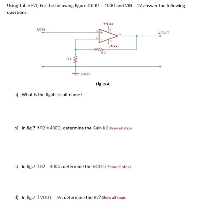
Transcribed Image Text:Using Table P.1, For the following figure 4 if R1 = 1000 and VIN = 1V answer the following
questions:
+Vee
VIN
υουT
Vee
ww.
R2
R1
GND
Fig. p.4
a) What is the fig.4 circuit name?
b) In fig.7 if R2 = 4000, determine the Gain K? Show all steps
c) In fig.7 if R2 = 4000, determine the VOUT? Show all steps
d) In fig.7 if VOUT = 6V, determine the R2? Show all steps
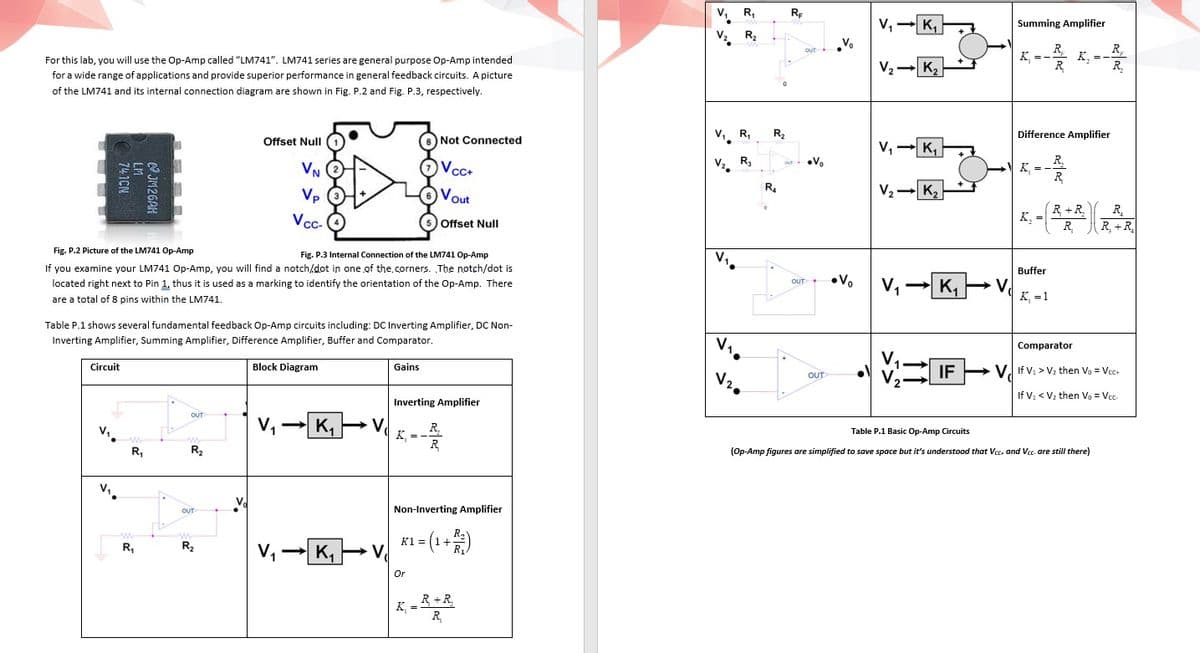
Transcribed Image Text:v, R,
RE
V, - K,
Summing Amplifier
V2 R2
R,
K, =-
R,
K, =-
R.
For this lab, you will use the Op-Amp called "LM741". LM741 series are general purpose Op-Amp intended
V2- K2
for a wide range of applications and provide superior performance in general feedback circuits. A picture
of the LM741 and its internal connection diagram are shown in Fig. P.2 and Fig. P.3, respectively.
V, R,
R,
Difference Amplifier
Offset Null
Not Connected
V, - K,
VN
V2.
R3
K, = -
R
R.
Vp
Vout
V2
K2
R.
Vc-
Offset Null
K,
R
Fig. P.2 Picture of the LM741 Op-Amp
Fig. P.3 Internal Connection of the LM741 Op-Amp
If you examine your LM741 Op-Amp, you will find a notch/dot in one of the.corners. The notch/dot is
Buffer
V,
K,
V
|K =1
located right next to Pin 1, thus it is used as a marking to identify the orientation of the Op-Amp. There
OUT
are a total of 8 pins within the LM741.
Table P.1 shows several fundamental feedback Op-Amp circuits including: DC Inverting Amplifier, DC Non-
Inverting Amplifier, Summing Amplifier, Difference Amplifier, Buffer and Comparator.
Comparator
Circuit
Block Diagram
Gains
→ V. If V. > V2 then Va = Voc+
OUT
If V; < V; then Vg = Vcc-
Inverting Amplifier
OUT
V,
- K,
R.
K =
Table P.1 Basic Op-Amp Circuits
R,
R2
(Op-Amp figures are simplified to save space but it's understood that Vec, and Vec. are still there)
OUT
Non-Inverting Amplifier
(1-
K1 =
R,
R2
V -
→ K.
→ V.
Or
R +R.
K, =
R,
JM26AH
741CN
Expert Solution
This question has been solved!
Explore an expertly crafted, step-by-step solution for a thorough understanding of key concepts.

Step by step
Solved in 2 steps with 2 images

Knowledge Booster


Learn more about
Need a deep-dive on the concept behind this application? Look no further. Learn more about this topic, electrical-engineering and related others by exploring similar questions and additional content below.Recommended textbooks for you
Introductory Circuit Analysis (13th Edition)
Electrical Engineering
ISBN:
9780133923605
Author:
Robert L. Boylestad
Publisher:
PEARSON

Delmar's Standard Textbook Of Electricity
Electrical Engineering
ISBN:
9781337900348
Author:
Stephen L. Herman
Publisher:
Cengage Learning

Programmable Logic Controllers
Electrical Engineering
ISBN:
9780073373843
Author:
Frank D. Petruzella
Publisher:
McGraw-Hill Education
Introductory Circuit Analysis (13th Edition)
Electrical Engineering
ISBN:
9780133923605
Author:
Robert L. Boylestad
Publisher:
PEARSON
Delmar's Standard Textbook Of Electricity
Electrical Engineering
ISBN:
9781337900348
Author:
Stephen L. Herman
Publisher:
Cengage Learning
Programmable Logic Controllers
Electrical Engineering
ISBN:
9780073373843
Author:
Frank D. Petruzella
Publisher:
McGraw-Hill Education

Fundamentals of Electric Circuits
Electrical Engineering
ISBN:
9780078028229
Author:
Charles K Alexander, Matthew Sadiku
Publisher:
McGraw-Hill Education

Electric Circuits. (11th Edition)
Electrical Engineering
ISBN:
9780134746968
Author:
James W. Nilsson, Susan Riedel
Publisher:
PEARSON

Engineering Electromagnetics
Electrical Engineering
ISBN:
9780078028151
Author:
Hayt, William H. (william Hart), Jr, BUCK, John A.
Publisher:
Mcgraw-hill Education,