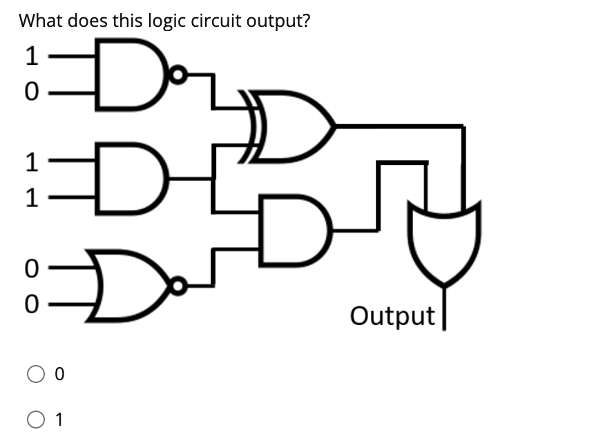
What does this logic circuit output? 1 1 1 Output O 1


Q: Q1/ Draw the logic circuit after simplify the circuit show below using K. map: B Y
A: First we will convert the above circuit into its POS form which is Y=A+B+C·A+B+C·A+B+C
Q: Design a combinational logic circuit with four inputs (a,b,c,d) and one output F. It has the…
A:
Q: 3. Build the logic circuit for the following function using Programmable Logic Array (PLA). F1 = ABC…
A: A programmable logic controller (PLC) or programmable controller is a ruggedized and modified…
Q: Q. 1 Implement the logic circuit for the following expression of Y. Y = Ā.B + C.B
A: As per the guidelines of Bartleby we supposed to answer first question only.
Q: 24) 24) Neatly draw the logic circuit for the expression below. Do not minimize or change the…
A: 24. We draw the given expression as follows.
Q: Derive the state table and the state graph for the following logic circuit: A' B' B DA Clock Clock X…
A: The solution is given below
Q: The combinational logic circuit includes a memory device True False
A: In this answer we will try to analyse whether the given statement is true or false.
Q: 5.1 Draw the logic diagram for a D FF using only NOR gates. 5.2 The waveform shown below is…
A: 5.1 D ff using NOR gates
Q: What is the final full formula? Minterm- F=C’D+A’B’D+ABD Maxterm-…
A: F=C’D+A’B’D+ABD
Q: what is the name of this formula Td = 1/2f
A: propositional logic formula: In formal logic, a propositional formula could be a form of…
Q: * For the logic circuit shown below FA F F=AB O F=A'+B' O F=A+B O F=AB'+A'B O ABO
A: In this answer we will find the resultant expression of F as explained below.
Q: Draw the logic circuit for the following expressions : a) AB + AB b) AB + AB+ ABC c)AB(C + D) d) A +…
A:
Q: Fill in the truth table below. Draw the Karnaugh map and show it in its simplest form. Draw the…
A:
Q: Q2:Draw the logic circuit to Storage the data (110110).
A: As per the guideline we need to solve only first question. we need to draw the logic circuit to…
Q: نقطة واحدة * For the logic circuit shown below A B FA F F=AB'+A'B F=AB F=A+B F=A'+B' O
A:
Q: Q1. Design a 4-input, one output combinational logic circuit for the following input-output…
A:
Q: Prove the logic equality A. (B+C) = A· B+ A B C
A: Given: A·(B+C)=A·B+A·B¯·C
Q: A logic function f(A,B,C) implemented with 4x1 MUX circuit. Implement the same function with using…
A:
Q: Need kmap foR TT ALSO DRAW LOGIC DIAGRAM OF TT
A: According to the question, for the given truth table as shown below we need to design K-Map and…
Q: Consider the multiplexer based logic circuit shown in the figure w MUX MUX ·F 1 Select one: O a. W…
A: Given diagram,
Q: Construct the logic circuit for X = AB(B’+C).
A: Given that BOOLEN expression X = AB(B’+C). Here X is the overall out put function Inputs are A,B,C…
Q: Q1/ Logic devices divide into two major types: what are they ? Briefly.
A: Logic devices are divided into two major categories. They are a) Fixed b) Programmable
Q: 28 Draw a logic circuit that will accomplish the equation F= [(A+C ·B) + A ·B·T] · (B+ C)
A: Given data, The expression for function is given as, F=(A+C·B')+A·B'·C'·B+C' The logic…
Q: 6. For the follow logic circuit system, the output f is: 5 (A) ab. (B) a + b. (C) a'+b'. (D) "E a bo
A: Option - B ( Answer )
Q: Simplify the logic diagram below. А Out A B
A: The solution can be achieved as follows.
Q: The simplified form of a logic function Y = A(B+C(AB+ AC)) will be
A:
Q: Write the result in the minimum SOP form from the Karnaugh map Digital Logic Circuits university…
A: The solution is given below
Q: Draw the logic diagram
A:
Q: Question 2 By using 4 to 1 MUX, Design a logic circuit that use to detect the month exceed thirty…
A: Mux is also known as a multiplexer which is used to send more data through single transmission. Also…
Q: The logic gate is the most basic building block of ____________ circuits A) None of the given…
A: Choose the correct option The given statement The logic gate is the most basic building block of…
Q: 6. For the follow logic circuit system, the output f is: [ (A) ab. (B) a + b. (C) a'+b'. (D) a'b' a…
A: Given, The logic circuit is,
Q: Draw the logic diagrams for the following Boolean expressions: (a) Y= A'B' +B (A+ C) (b) Y= BC +AC…
A:
Q: Q3) Draw a logic circuit for the following: a) x'y'z' + xy + Xz + y'z
A:
Q: 2.3 A logic signal is required to give an indication when: a. the supply to an oven is on, and b.…
A: The indication is required for the following: The supply to the oven is on and the temperature of…
Q: Q2 / Sketch the logic circuit described by the following expression: Y= [ (AB) O (C +B) e D] Z
A: So we need the equivalent logic circuit.
Q: Draw the logic diagrams for the following Boolean expressions: (a) Y=A'B' +B (A+ C) (b) Y= BC + AC'…
A: As mentioned by the student we have to solve the questions c and d.
Q: Design a logic circuit that controls the passage of a signal A according to the following…
A: In this question we design a logic circuit that controls the passage of a signal A according to the…
Q: Given a 2 input-4 column 3-output programmable logic array (PLA) device as shown in Figure Q2(e).…
A:
Q: How can I create a circuit based on the table below, I have 2 inputs and 2 outputs. I would like to…
A:
Q: A single logic gate in a prototype integrated circuit is found to be capable of switching from the…
A:
Q: Draw the logic circuit represented by each of the following expre- • AB + AB ● AB(CD + EF)
A: In this question we will draw logic circuit represented by given expressions....
Q: F1Β (A' + AC) F2 = (A+ C')(B + B'C') A В F1 F2
A:
Q: Z= (A+B + CDE)+ B CD
A: The function is given as, Z=A+B+C-DE-+B-CD-
Q: Below is an NMOS logic circuit. For all of the MOSFETs assume V = 1 V and k = 50 mA/V². th 5V 5V R₂…
A: Given question is related to logic family circuits
Q: A. B C- Logic circuits for each of given below : (i) (A+B)C + B (ii) (A+B)C (iii) ABC + AB (iv) A+ B…
A:
Q: Q91 For the Logic Circuit shown in figure (6) write the SOP logical expression of the function (F)…
A:
Q: Convert the given table into a logic diagram. Upload a photo of your output showing your solution.…
A: 2421 code is the Aiken code it is the complementary BCD code. In this Aiken code the four bits are…
Q: Question 1 Simplify a logic function F(a,b,c,d) = a'b'cd + a'bd + bc'd' + ab'c'ď assuming that the…
A: It is a 4 variable k map hence we will have 16 combination of inputs. We must insert all the…

Step by step
Solved in 2 steps


- The basic circuit of a TTL gate is shown in thecircuit of Figure P10.49. Determine the logic functionperformed by this circuit.How to do ? Need *State diagram *State/output table *Transition table *Transition equation *Excitation equation and output equation *Logic circuit diagramHow to do ? Need *State/output table *Transition table *Transition equation *Excitation equation and output equation *Logic circuit diagram
- Write an assembly language program for 8085 microprocessor to add 2 digit BCD numbers stored in memory location C050H and C051H respectively and store the result in memory location C052H.Develop the logic required to detect the binary code 10010 and produce an active-Low outputAssume Vth = 1V and k = 50mA/V2. Given the schematic below, do the following: 1) Indicate and verify the state of each MOSFET and ?0 for the following input combinations. Fill-out the table below for each assumed state of the MOSFET for every input combination. Use ?ds,on approximation for linear operation. 2) Determine what kind of logic circuit is implemented in the circuit.
- The power supply −VEE as shown is changed to−2 V. What are the new values of REE and RC1required to keep the logic levels and logic swingunchanged? What is the new power dissipation?Digital Electronics and Design Questiona) Find the logic function ‘F’ realized by the CMOS circuit below. b) Complete the missing logic signals in the circuit. c) Write the Verilog HDL or VHDL code that implements the logic function.The initial state of the four-bit synchronous binary addition counter Q3Q2Q1Q0 is 1100. After 8 CP clock pulses, its state Q3Q2Q1Q0 changes to ----?
- 1) Draw how an ASIC, SOC, MCU, MPU, DSP any TTL gates of the TTL circuits you have constructed or designed to use a transistor (BJT/MOS) to drive the current specification of a LOAD (ie RELAY, Motor, Light array of High powered LEDs)Draw the the basic logic diagram of decimal to BCD Encoder .DESIGN A CIRCUIT THAT ADDS AN 8-BIT BINARY NUMBER TO ANOTHER 8-BIT BINARY NUMBER USING THE IC 74283 AND ANY OTHER GATES