1. Determine the Boolean Function of the C, D, E, F, G nodes for the circuit given in Figure 1. D. 4700 4700 4.7k 4700 4.T. 470 470 Figure 1: Cireuit 1 Iculate the truth table of this circuit and fill in Table 1. в A' B' D E G Table 1: Truth table of the cireuit in Figure 1 1. Draw the circuit in Proteus and put a screenshot of the work. . Simplify the output of this circuit (G) using basic identities of Boolean Algebra and plot the simplified circuit. Do not u simplification. Calculate the truth table of this simplified circuit and fill in Table 2.
1. Determine the Boolean Function of the C, D, E, F, G nodes for the circuit given in Figure 1. D. 4700 4700 4.7k 4700 4.T. 470 470 Figure 1: Cireuit 1 Iculate the truth table of this circuit and fill in Table 1. в A' B' D E G Table 1: Truth table of the cireuit in Figure 1 1. Draw the circuit in Proteus and put a screenshot of the work. . Simplify the output of this circuit (G) using basic identities of Boolean Algebra and plot the simplified circuit. Do not u simplification. Calculate the truth table of this simplified circuit and fill in Table 2.

Chapter4: Processor Technology And Architecture
Section: Chapter Questions
Problem 9VE

Related questions
Question
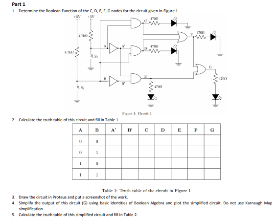
Transcribed Image Text:Part 1
1. Determine the Boolean Function of the C, D, E, F, G nodes for the circuit given in Figure 1.
+5V
+5V
470
470
4.7k
4700
4.7k
4700
(S
4702
Figure 1: Cireuit 1
2. Calculate the truth table of this circuit and fill in Table 1.
A
в
A'
B'
D
E
F
G
1
1
1
1
Table 1: Truth table of the circuit in Figure 1
3. Draw the circuit in Proteus and put a screenshot of the work.
4. Simplify the output of this circuit (G) using basic identities of Boolean Algebra and plot the simplified circuit. Do not use Karnaugh Map
simplification.
5. Calculate the truth table of this simplified circuit and fill in Table 2.
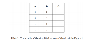
Transcribed Image Text:A
B
G
1
Table 2: Truth table of the simplified version of the circuit in Figure 1
Expert Solution
This question has been solved!
Explore an expertly crafted, step-by-step solution for a thorough understanding of key concepts.

Step by step
Solved in 2 steps with 1 images

Knowledge Booster


Learn more about
Need a deep-dive on the concept behind this application? Look no further. Learn more about this topic, computer-science and related others by exploring similar questions and additional content below.Recommended textbooks for you
Systems Architecture
Computer Science
ISBN:
9781305080195
Author:
Stephen D. Burd
Publisher:
Cengage Learning
Systems Architecture
Computer Science
ISBN:
9781305080195
Author:
Stephen D. Burd
Publisher:
Cengage Learning