1. Figure 1 shows the partial datasheet for a 2N5458 JFET. Based on datasheet in Figure I obtain the value of typical Inss and maximum Vosom Use these values to calculate the drain current for Vos -0 V, -2 V, and -3 V. 2. JFET biasing is used to select the proper de gate-to-source voltage to establish a desired value of drain current and thus a proper Q-point. To illustrate JFET biasing circuit, sketch the self-biased n-channel JFET. If the given the parameter values of lb-8 mA, Rp = 2.0 ka, Ra = 10 MN, Rs = 280 2 and VDD =24 V, determine Vps and Vos
1. Figure 1 shows the partial datasheet for a 2N5458 JFET. Based on datasheet in Figure I obtain the value of typical Inss and maximum Vosom Use these values to calculate the drain current for Vos -0 V, -2 V, and -3 V. 2. JFET biasing is used to select the proper de gate-to-source voltage to establish a desired value of drain current and thus a proper Q-point. To illustrate JFET biasing circuit, sketch the self-biased n-channel JFET. If the given the parameter values of lb-8 mA, Rp = 2.0 ka, Ra = 10 MN, Rs = 280 2 and VDD =24 V, determine Vps and Vos

Delmar's Standard Textbook Of Electricity
7th Edition
ISBN:9781337900348
Author:Stephen L. Herman
Publisher:Stephen L. Herman
Chapter29: Dc Generators
Section: Chapter Questions
Problem 1PA: You are working as an electrician in a large steel manufacturing plant, and you are in the process...

Related questions

Question
Answer question 1 and 2 in 30 minute

Transcribed Image Text:1. Figure 1 shows the partial datasheet for a 2N5458 JFET. Based on datasheet in Figure
1 obtain the value of typical Ipss and maximum VGs(om Use these values to calculate
the drain current for Vos -0 V, -2 V, and -3 V.
2. JFET biasing is used to select the proper de gate-to-source voltage to establish a desired
value of drain current and thus a proper Q-point. To illustrate JFET biasing circuit,
sketch the self-biased n-channel JFET. If the given the parameter values of Ip - 8 mA,
Rp = 2.0 ka, Rg = 10 MQ, Rs = 280 2 and Vpp =24 V, determine Vps and Vos
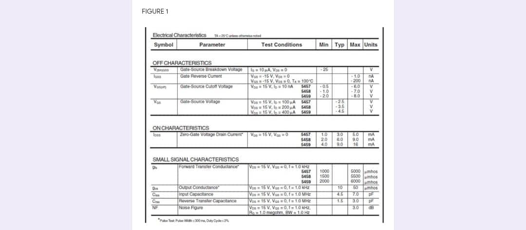
Transcribed Image Text:FIGURE 1
Electrical Characteristics
TA2Ciethurated
Symbol
Min Typ Max Units
Туp Маx |Units
Parameter
Test Conditions
OFF CHARACTERISTICS
Vas
-25
Gate-Source Breakdown Voltage
Gate Reverse Current
la = 10A, Vos =0
Von =-15 V, Voe =0
Vos = -15 V, Ves =0, Ta 100'C
Vog= 15 V. e = 10 NA
lass
1.0
-200
-6.0
-7.0
-8.0
nA
nA
Vasn
Gate-Source Cutoff Voltage
5457
5458
5459
0.5
- 1.0
-20
V
Vos
Gate Source Voitage
Vos = 15 V, le = 100 A
Vos = 15 V, lo= 200 A
Von 15 V, = 400 A 5459
-25
-3.5
4.5
5457
5450
ONCHARACTERISTICS
Zero-Gate Voltage Drain Currenit
Vos = 15 V, Vas = 0
6.0
9.0
16
loss
5457
1.0
5458
S450
20
4.0
3.0
6.0
9.0
mA
mA
SMALL SIGNAL CHARACTERISTICS
Forward Transter Conductarice
Vos= 15 V, Vos =0,1=1.0 KHZ
5457
5000 umhos
5500 umhos
6000 mhos
50 umhos
7.0 pF
3.0 DF
3.0
5458
5459
1000
1500
2000
Output Conductance
input Capacitance
Reverse Transter Capacitance
Vos = 15 V, Vas =0,1= 1,0 kHZ
Vos = 15 V, Vas =0, =1.0 MHE
Vos = 15 V, Vos =0, 1= 1.0 MH2
Von = 15 V, Vos = 0,1= 1.0 KHZ.
Re 1.0 megchm. BW = 1.0 Hz
10
Cas
4.5
1.5
Csa
NF
Noise Figure
* et WMah300 m, Dy Cyes
Expert Solution
This question has been solved!
Explore an expertly crafted, step-by-step solution for a thorough understanding of key concepts.

Step by step
Solved in 3 steps with 2 images

Knowledge Booster


Learn more about
Need a deep-dive on the concept behind this application? Look no further. Learn more about this topic, electrical-engineering and related others by exploring similar questions and additional content below.Recommended textbooks for you
Delmar's Standard Textbook Of Electricity
Electrical Engineering
ISBN:
9781337900348
Author:
Stephen L. Herman
Publisher:
Cengage Learning


Power System Analysis and Design (MindTap Course …
Electrical Engineering
ISBN:
9781305632134
Author:
J. Duncan Glover, Thomas Overbye, Mulukutla S. Sarma
Publisher:
Cengage Learning
Delmar's Standard Textbook Of Electricity
Electrical Engineering
ISBN:
9781337900348
Author:
Stephen L. Herman
Publisher:
Cengage Learning
Power System Analysis and Design (MindTap Course …
Electrical Engineering
ISBN:
9781305632134
Author:
J. Duncan Glover, Thomas Overbye, Mulukutla S. Sarma
Publisher:
Cengage Learning