1.1. Which of the following are true about MOSFET devices? (a) MOS stands for "Metallurgy Of Semiconductors" (b) MOSFET current conduction is due to drift phenomenon (c) An externally induced voltage at the gate is fundamental to inversion layer (d) Naming of "Source" and "Drain" regions are only dependent on aspect ratio 1.2. Which of the following are true about NMOS transistors (a) The threshold voltage can be positive or negative depending on geometry (b) Channel length modulation parameter (A) is always positive (c) Current flows from drain to source (d) Threshold voltage is a fixed value based on process, it cannot be changed by external voltages 1.3. In a MOS device (a) Cas and Cap both have both geometry and voltage dependencies (b) Cas is takes minimum value at saturation while Cco goes to maximum value (c) Cos and Csa are contributed from reverse bias p-n diode formation (d) High frequency gain of an amplifier is independent of intrinsic capacitors 1.4. For an NMOS device (a) The DC component of input current has almost zero value (b) The AC component of input current has a finite value (c) Small signal parameters are derived first independent of large signal parameters and are tweaked for best performance (d) DC operating points are first fixed and small signal values are uniquely computed
1.1. Which of the following are true about MOSFET devices? (a) MOS stands for "Metallurgy Of Semiconductors" (b) MOSFET current conduction is due to drift phenomenon (c) An externally induced voltage at the gate is fundamental to inversion layer (d) Naming of "Source" and "Drain" regions are only dependent on aspect ratio 1.2. Which of the following are true about NMOS transistors (a) The threshold voltage can be positive or negative depending on geometry (b) Channel length modulation parameter (A) is always positive (c) Current flows from drain to source (d) Threshold voltage is a fixed value based on process, it cannot be changed by external voltages 1.3. In a MOS device (a) Cas and Cap both have both geometry and voltage dependencies (b) Cas is takes minimum value at saturation while Cco goes to maximum value (c) Cos and Csa are contributed from reverse bias p-n diode formation (d) High frequency gain of an amplifier is independent of intrinsic capacitors 1.4. For an NMOS device (a) The DC component of input current has almost zero value (b) The AC component of input current has a finite value (c) Small signal parameters are derived first independent of large signal parameters and are tweaked for best performance (d) DC operating points are first fixed and small signal values are uniquely computed

Introductory Circuit Analysis (13th Edition)
13th Edition
ISBN:9780133923605
Author:Robert L. Boylestad
Publisher:Robert L. Boylestad
Chapter1: Introduction
Section: Chapter Questions
Problem 1P: Visit your local library (at school or home) and describe the extent to which it provides literature...

Related questions
Question
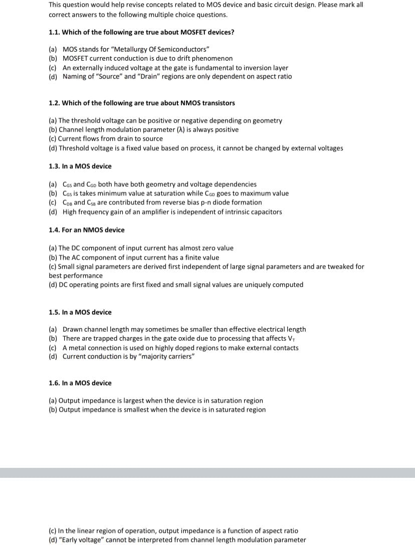
Transcribed Image Text:This question would help revise concepts related to MOS device and basic circuit design. Please mark all
correct answers to the following multiple choice questions.
1.1. Which of the following are true about MOSFET devices?
(a) MOS stands for "Metallurgy Of Semiconductors"
(b) MOSFET current conduction is due to drift phenomenon
(c) An externally induced voltage at the gate is fundamental to inversion layer
(d) Naming of "Source" and "Drain" regions are only dependent on aspect ratio
1.2. Which of the following are true about NMOS transistors
(a) The threshold voltage can be positive or negative depending on geometry
(b) Channel length modulation parameter (A) is always positive
(c) Current flows from drain to source
(d) Threshold voltage is a fixed value based on process, it cannot be changed by external voltages
1.3. In a MOS device
(a) Cas and CGp both have both geometry and voltage dependencies
(b) Cas is takes minimum value at saturation while CGD goes to maximum value
(c) CoB and Cse are contributed from reverse bias p-n diode formation
(d) High frequency gain of an amplifier is independent of intrinsic capacitors
1.4. For an NMOS device
(a) The DC component of input current has almost zero value
(b) The AC component of input current has a finite value
(c) Small signal parameters are derived first independent of large signal parameters and are tweaked for
best performance
(d) DC operating points are first fixed and small signal values are uniquely computed
1.5. In a MOS device
(a) Drawn channel length may sometimes be smaller than effective electrical length
(b) There are trapped charges in the gate oxide due to processing that affects V,
(c) A metal connection is used on highly doped regions to make external contacts
(d) Current conduction is by “majority carriers"
1.6. In a MOS device
(a) Output impedance is largest when the device is in saturation region
(b) Output impedance is smallest when the device is in saturated region
(c) In the linear region of operation, output impedance is a function of aspect ratio
(d) "Early voltage" cannot be interpreted from channel length modulation parameter
Expert Solution
This question has been solved!
Explore an expertly crafted, step-by-step solution for a thorough understanding of key concepts.

This is a popular solution!

Trending now
This is a popular solution!

Step by step
Solved in 2 steps

Recommended textbooks for you
Introductory Circuit Analysis (13th Edition)
Electrical Engineering
ISBN:
9780133923605
Author:
Robert L. Boylestad
Publisher:
PEARSON

Delmar's Standard Textbook Of Electricity
Electrical Engineering
ISBN:
9781337900348
Author:
Stephen L. Herman
Publisher:
Cengage Learning

Programmable Logic Controllers
Electrical Engineering
ISBN:
9780073373843
Author:
Frank D. Petruzella
Publisher:
McGraw-Hill Education
Introductory Circuit Analysis (13th Edition)
Electrical Engineering
ISBN:
9780133923605
Author:
Robert L. Boylestad
Publisher:
PEARSON
Delmar's Standard Textbook Of Electricity
Electrical Engineering
ISBN:
9781337900348
Author:
Stephen L. Herman
Publisher:
Cengage Learning
Programmable Logic Controllers
Electrical Engineering
ISBN:
9780073373843
Author:
Frank D. Petruzella
Publisher:
McGraw-Hill Education

Fundamentals of Electric Circuits
Electrical Engineering
ISBN:
9780078028229
Author:
Charles K Alexander, Matthew Sadiku
Publisher:
McGraw-Hill Education

Electric Circuits. (11th Edition)
Electrical Engineering
ISBN:
9780134746968
Author:
James W. Nilsson, Susan Riedel
Publisher:
PEARSON

Engineering Electromagnetics
Electrical Engineering
ISBN:
9780078028151
Author:
Hayt, William H. (william Hart), Jr, BUCK, John A.
Publisher:
Mcgraw-hill Education,