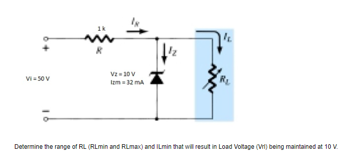
1k Vi = 50 V Vz = 10 V Izm = 32 mA etermine the range of RL (RLmin and RLmax) and ILmin that will result in Load Voltage (Vrl) being
Q: Calculate Drain current and VGS for the JFET with voltage divider bias. Given VDD = 12V, VD = 7V, R1…
A: JFET problem can be solved easily.
Q: Determine the output voltage in terms of v1 and v2. 1.0V 1ka 4kQ A-35.0V 741 1ka 1ka 수-35.0V V2s 1V…
A:
Q: Determine VGs (in Volts) for the JFET with voltage-divider bias in the figure, given that for this…
A: By given details first we will find out gate voltage then drain then source voltage then we will…
Q: Calculate the output voltage using the circuit of figure below for resistor components of value…
A: The amplifier is an electronic device whose output is amplified version of the input signal. The…
Q: An n-chan nannel JFEI With voltage-divider bias has a gate voltage of 3 V and a source . voltage Of…
A:
Q: 4. Given the voltage-divider bias configuration below and the voltage between collector and ground…
A: Bipolar Junction Transistor: A BJT is a current controlled device in which output is controlled by…
Q: Design the circuit shown to obtain a dc voltage of +0.15 V at each of the drains of Q₁ and Q when…
A: Transistor:- It is a three terminal device that is used to amplify the input signal or regulate…
Q: 1. Write the types of transistors in each circuit in the figure and in which supply region they are.…
A: four types of figure
Q: If Vcc = +18 V, voltage-divider resistor R₁ is 4.7 kg, and R₂ is 1500, what is the base bias…
A:
Q: Q1: VDD +12 V Determine Ip and VGs for the JFET with voltage-divider bias in Figure 1, given that…
A: The solution is given below
Q: DIA and A/D Converters VR Sw Sw2 Swa SwA : 2R 2R 2R 2R R ww ww 2R www R R. R b4 by b2 b1 The…
A: DAC and ADC are data converters. A ADC(analog to digital converter) circuit convert analog data in…
Q: Izwe 2 KJL 10 Me 2Mr 12v Ia 6 mA - 5V Compute Q-point (Vps and Ip) for this N-channel JFET circuit O…
A: In this question, We need to choose the correct options What is Q point of the given circuit?
Q: 20 V = 2.5 mA IDQ RD VD=12 G I Dss =6 m Vp =-3 V
A:
Q: '- What the range of developed output voltage for the circuit of figure below if the 1= 0.0067 mA,…
A: In the given circuit If=I1+I2+I3If=0.0067+0.023+0.067If=0.0967 mA Case (1) when variable resistance…
Q: Calculate the output voltage using the circuit of figure below for resistor components of value…
A: Amplifier is an electronic device whose output is amplified version of the input signal. The…
Q: Solve the base current (IB) of Figure 611. VCC 18V R2 3.9kQ R1 680KQ Vc = 8V Figure 611
A:
Q: +1 L₁ C1 2 L2 m C₂. www RL + Vo I
A: Solution
Q: ider an npn transistor with VBE = 0.7 V at iċ = 1 mA. Find VBE at ic = 0.1 mA and 10 n
A:
Q: Find the region of operation and drain current in aPMOS transistor with W/L = 20/1 for VBS = 0 Vand…
A: Given data is as follows; WL=201 ,VBS=0 V a) We will consider for…
Q: Determine Voltage gain v/v, in Figure 8.4. 60 k2 ww 30 k2 ww 50 k2 RL ww 20 kN ww
A: This question belongs to analog electronics . It is based on the concept of virtual ground and…
Q: 2. a) Define the function of each opamp given below. b) Calculate V.. 18K ww 36K 6K 6K 2 V Div 12K…
A:
Q: Q1) For the following system, find the state space model. Consider vi input, vo output. Choose…
A:
Q: Determine the Thevenin resistance for the bias netw Vcc = 12 V 2k 65k €200 www 10k Σ Select one: O…
A: In this question, We need to choose the correct options What is the Thevenin resistance of the bias…
Q: The Si transistor of the following figure has a-0.99, VEE= 4V and Vc=12V. i- If I-1.1 mA, find Ry.…
A: Given circuit: α=0.99VEE=4 VVCC=12 VIE=1.1 mAVCE=-7 V
Q: With a voltage divider bias circuit calculate the value of base current with R1 = 20.9 kΩ, R2 = 30…
A: The diodes are made of semiconductor materials. Silicon and germanium are common semiconductors for…
Q: eran V+ RC Ry Cc2 Rs RL CCI R21 CE RE hommas gravy c Vout RL Rc DATA (D:) ww.
A: For ac model of transistor dc must be short circuited and coupling capacitors must be opened.
Q: 20 k2 50 kΩ 30 k2 ww 10 k2 /2
A: Operational Amplifier: A direct coupling amplifier that can increase the bandwidth of an input…
Q: VCC 20V 39KQ 3.3kQ •VC VB - VE 8.2kQ 1.0kQ Figure 6.3 Voltage divider bias
A: This is a basic problem of bjt The solution is shown in the next step
Q: 8) For a source follower type voltmeter r= 10 k, gm=0.003 mho, R, = 15 kand R = 1800. How much…
A: Given values: rd= 10 kΩ, gm=0.003 mho, Rs=15 kΩRm=1800 Ω, Vin= 1 V
Q: The npn transistor circuit of Figure 1 has VBE = 0.5 V and Bp = 80. Determine the value of R1 that…
A: The solution is given below
Q: A battery with EMF of 4V and an internal resistance, r = 0.80 is connected to a load resistance R =…
A:
Q: A power supply can deliver a maximum rated current of 0.5 A at full-load output voltage of 20 V.…
A:
Q: learly identify/label all node voltages including reference node. Write clearly all required KCL…
A:
Q: Find the labeled values, consider β = 100 and | Vbe | = 0.7V
A: Given: In the given question they have mentioned a common emitter amplifier configuration circuit.…
Q: QUESTION 9: The circuit parameters are V*= 10.5 V, V = -10.5 V, Io= 0.5 mA, and Rc = 9 kN. The…
A: The transistor is a three-terminal device used for the regulation of signals. It is used for…
Q: What is the required input voltage (volts) for a wheatstone bridge to produce an output voltage of…
A: The Wheatstone bridge with the given values is shown below: The output voltage is the voltage…
Q: +V¢ 오 RC Ic RB IB. Vi H IE
A:
Q: self -bias netwrk using JFET transistor with IDss =8mA and Vp = -6V to have a IDQ = 4mA using supply…
A:
Q: Design Vo Itage Regulator will maintain output vo ltage of 20v acnss IK loadwith on in put that will…
A:
Q: 50 ) 25 V + 10Ω + 1)
A:
Q: For a particular FET, Ip(on) = 190mA at VGs = 5 V, VGs(th) = 3 V. Find the the drain current Ip at…
A: FET is a field effect transistor. In this device, the electric field is developed and this controls…
Q: Q2) Determine Zi, Zo, and Av for the network of figure below (let Vaso -1.5 V). ISV +IN V I MO loss…
A: JFET(Junction -gate field -effect Transistor) is three terminal electronic device. Three terminal…
Q: VDD Rp Cc Q2 Cc RL RG Rs For the series-connected identical JFETs of Figure above, IDSS = 8 mA and…
A: BJT and MOSFET are the class of transistors used in analog electronics. They are widely used…
Q: Q2 /A)- What the range of developed output voltage for the circuit of .figure below if the 1= 0.0067…
A: Output voltage range of inverting op amplifier. Feedback element is variable. V+ = V- = 0V using…
Q: Calculate the total offset voltage for the circuit of the figure below with specified values of…
A: The output offset voltage due to input offset voltage is given by Voff = (1 + Rf/R1) Vio Given Rf…
Q: The circuit and transistor parameters are given as follows: B= 130, lco 0.2 mA, VA= 80 V, V,-1 V,…
A: Given data, β=130ICQ=0.2mAVA=80VVi=1VV+=3.3VR1=150kΩR2=5kΩ
Q: For the circuits shown below, where the BJTS have ß=110, find Icı, Ic2, Ii, and Vo. (a) Vi = 0.4V,…
A: Here, we have given a circuit, for which the value of β. And, when Vi=0.4 V we have to calculate…
Q: D/A and A/D Converters Swi Sw2 Sws SwA 2R 2R 2R 2R www 2R R. R b2 by b4 The resistance Rf is…
A: DAC and ADC are data converters. A ADC(analog to digital converter) circuit convert analog data in…
Q: (h) Which of the circuits shown in Figure 1.8 will have an output current of -2.5 µA if a 1MN load…
A: Given data is input voltage VIN=5V, Resistor values R1=2kΩ, R2=1kΩ. And Load resistor RL=1MΩ…
Q: Q4. Determine the value of the base resistor () and the load resistor () in the circuit shown in…
A:
Step by step
Solved in 2 steps with 2 images
- Find the values of IC and VCE of the circuit shown in the figure below.Assume: β = 100, VCC = 15V, VBE = 0.7V, R1 = 50kΩ, R2 = 25kΩ, RC = 1kΩ andRE = 1kΩ.Find the IBQ, ICQ, VCE, VB, VC, VE and VBC values in the following transistor circuit. (β = 90, R1 = 560 kohm, R2 = 3.9 kohm)Design the following circuit so that the operating point is at the center of the load line, keep the value of Rx. Vcc=24V, Icmax=50mA. Draw the load line.Rx=15KΩβ =86.
- Since Vcc = 12 V, Vin = 171 mV, RB = 780 kΩ, RC1 = 12 Ω, RC2 = 3 Ω, RE = 470 Ω, RL = 47 Ω and β1 = β2 = 100 in the circuit in the figure, the current flowing through the load resistor RL (IL) find? NOTE-1: VBE1 = VBE2 = 0.7 V will be taken. NOTE-2: Output impedances of transistors (r0) will be neglected.Please solve the problem. Thank you (Electronics) Given zener voltage at 9V, input voltage at 12Vdc to 15Vdc and ILmax at 40mA. What is Rsmin if Izmaxrated is 50mA?Define also what is Rsmax? Choices: a) 43 ohms b)10 ohms c) 50 ohms d)20 ohmsWhat is the value of tP0 for a technology with L = 250 nm, n = 500 cm2/V-s,VDD = 3.3 V and VT N = VDD/4.
- Design the following circuit so that the operating point is at the center of the load line, keep the value of Rx. Vcc=24V, Icmax=50mA. draw the load line.What are the output current and output resistance of the current source as shown if Vo = VDD = 12 V, R4 = 680 kΩ, R3 = 330 kΩ, RS = 3 kΩ, Kn = 500 μA/V2, VT N = 0.7 V, and λ = 0.01 V−1?What is the output voltage for the circuit diagram given below? For VGS(on) = 4.5V , ID(on)=75mA , RDS(on) = 6ohm
- In a N-Channel JFET if the voltage across the drain and source (VDS) is increased then explain in detail with neat diagram the changes in drain current. Justify your answer.An NMOS transistor has the following values: Vto = 1V, KP = 50 x10-6A/V2, L= 5 x10⁻⁶m, and W= 50 x10-6m. For each set of voltages, state with reasons the region of operation and compute the drain current. i. VGS = 4V and VDS = 10V ii. VGS=4V and VDS =2V iii. VGS =0V and VDS = 10VConsider the following circuit. Calculate the output voltage when VGS=0 and VGS=-10V. Also, calculate the on-off ratio. PUT SUITABLE VALUE IN Vin