= 20 kHz. The 4.16 A bipolar transistor is operated as a chopper switch at a frequency of f, circuit arrangement is shown in Figure 4.47a. The de input voltage of the chopper is V = 400 V and the load current is IL tf = 4 µs. Determine the values of (a) L;; (b) C;; (c) R, for critically damped condition; (d) R, if the discharge time is limited to one-third of switching period; (e) R, if peak dis- charge current is limited to 5% of load current; and (f) power loss due to RC snubber P, neglecting the effect of inductor L, on the voltage of snubber capacitor C,. Assume that VCE(sat) = 125 A. The switching times are t, = 1.25 us and = 0.
= 20 kHz. The 4.16 A bipolar transistor is operated as a chopper switch at a frequency of f, circuit arrangement is shown in Figure 4.47a. The de input voltage of the chopper is V = 400 V and the load current is IL tf = 4 µs. Determine the values of (a) L;; (b) C;; (c) R, for critically damped condition; (d) R, if the discharge time is limited to one-third of switching period; (e) R, if peak dis- charge current is limited to 5% of load current; and (f) power loss due to RC snubber P, neglecting the effect of inductor L, on the voltage of snubber capacitor C,. Assume that VCE(sat) = 125 A. The switching times are t, = 1.25 us and = 0.

Introductory Circuit Analysis (13th Edition)
13th Edition
ISBN:9780133923605
Author:Robert L. Boylestad
Publisher:Robert L. Boylestad
Chapter1: Introduction
Section: Chapter Questions
Problem 1P: Visit your local library (at school or home) and describe the extent to which it provides literature...

Related questions
Question
Please solve it fast.
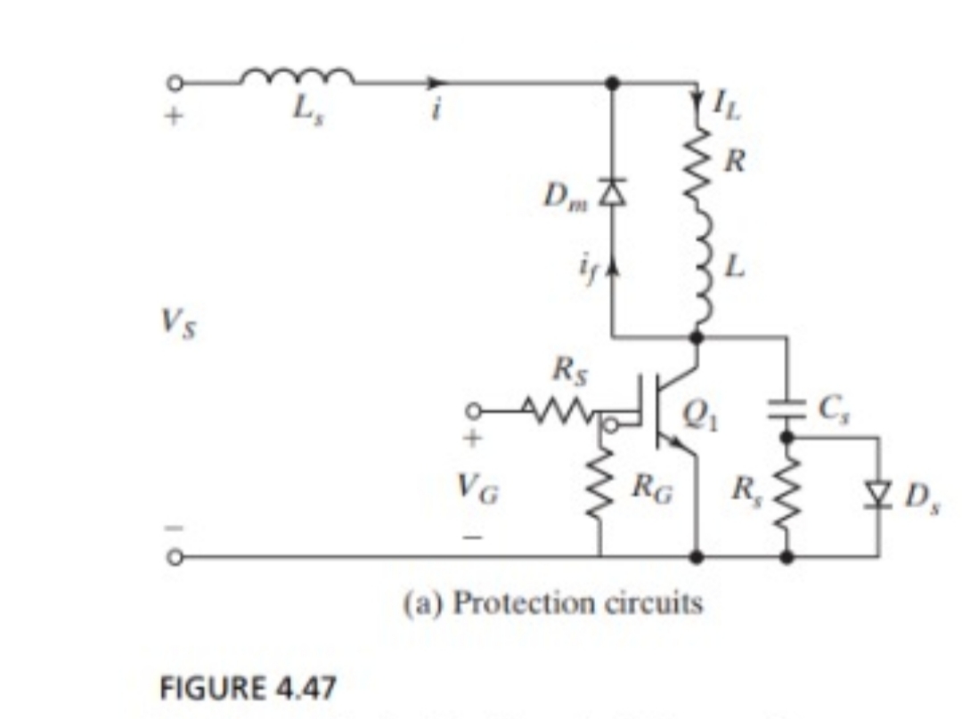
Transcribed Image Text:L,
i
Vs
Rs
VG
RG
R,
Y D,
(a) Protection circuits
FIGURE 4.47
Transcribed Image Text:= 20 kHz. The
4.16 A bipolar transistor is operated as a chopper switch at a frequency of f,
circuit arrangement is shown in Figure 4.47a. The de input voltage of the chopper is
V = 400 V and the load current is IL
tf = 4 µs. Determine the values of (a) L;; (b) C;; (c) R, for critically damped condition;
(d) R, if the discharge time is limited to one-third of switching period; (e) R, if peak dis-
charge current is limited to 5% of load current; and (f) power loss due to RC snubber P,
neglecting the effect of inductor L, on the voltage of snubber capacitor C,. Assume that
VCE(sat)
= 125 A. The switching times are t, = 1.25 µs and
= 0.
Expert Solution
This question has been solved!
Explore an expertly crafted, step-by-step solution for a thorough understanding of key concepts.

Step by step
Solved in 4 steps with 4 images

Knowledge Booster


Learn more about
Need a deep-dive on the concept behind this application? Look no further. Learn more about this topic, electrical-engineering and related others by exploring similar questions and additional content below.Recommended textbooks for you
Introductory Circuit Analysis (13th Edition)
Electrical Engineering
ISBN:
9780133923605
Author:
Robert L. Boylestad
Publisher:
PEARSON

Delmar's Standard Textbook Of Electricity
Electrical Engineering
ISBN:
9781337900348
Author:
Stephen L. Herman
Publisher:
Cengage Learning

Programmable Logic Controllers
Electrical Engineering
ISBN:
9780073373843
Author:
Frank D. Petruzella
Publisher:
McGraw-Hill Education
Introductory Circuit Analysis (13th Edition)
Electrical Engineering
ISBN:
9780133923605
Author:
Robert L. Boylestad
Publisher:
PEARSON
Delmar's Standard Textbook Of Electricity
Electrical Engineering
ISBN:
9781337900348
Author:
Stephen L. Herman
Publisher:
Cengage Learning
Programmable Logic Controllers
Electrical Engineering
ISBN:
9780073373843
Author:
Frank D. Petruzella
Publisher:
McGraw-Hill Education

Fundamentals of Electric Circuits
Electrical Engineering
ISBN:
9780078028229
Author:
Charles K Alexander, Matthew Sadiku
Publisher:
McGraw-Hill Education

Electric Circuits. (11th Edition)
Electrical Engineering
ISBN:
9780134746968
Author:
James W. Nilsson, Susan Riedel
Publisher:
PEARSON

Engineering Electromagnetics
Electrical Engineering
ISBN:
9780078028151
Author:
Hayt, William H. (william Hart), Jr, BUCK, John A.
Publisher:
Mcgraw-hill Education,