23-10: Derive the output logic equation F(x3,X2,X1,Xo) from the following circuit. Note that the priority of the priority encoder is I>Io>I3>I1. Priority 3-to-8 Encoder Decoder 0. 0. 0. 1 1 1 3. wwww 1 0 MUX 617 O123 0123
23-10: Derive the output logic equation F(x3,X2,X1,Xo) from the following circuit. Note that the priority of the priority encoder is I>Io>I3>I1. Priority 3-to-8 Encoder Decoder 0. 0. 0. 1 1 1 3. wwww 1 0 MUX 617 O123 0123

Chapter22: Sequence Control
Section: Chapter Questions
Problem 6SQ: Draw a symbol for a solid-state logic element AND.

Related questions
Question
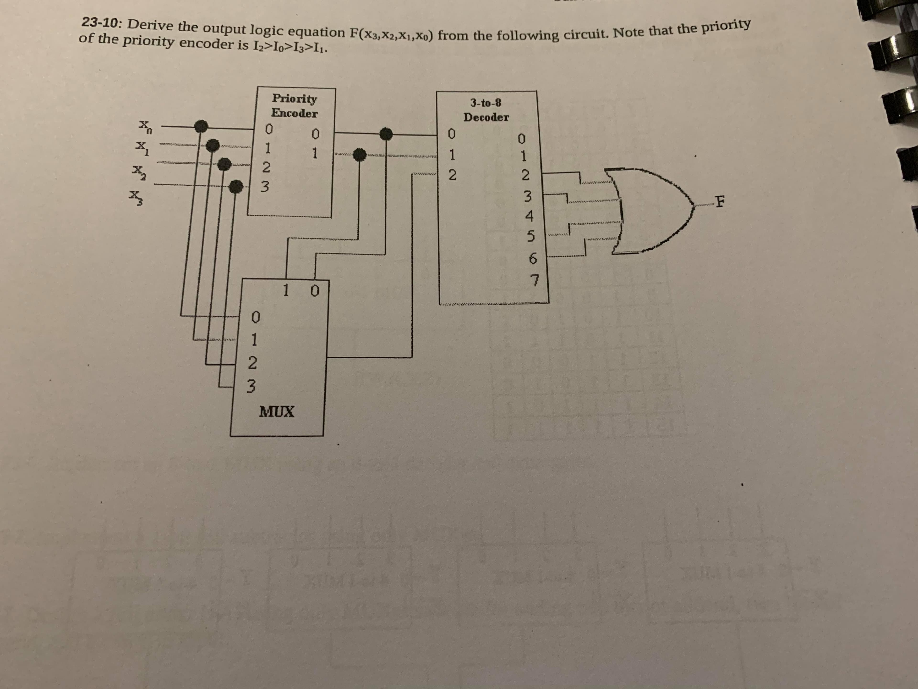
Transcribed Image Text:23-10: Derive the output logic equation F(x3,X2,X1,Xo) from the following circuit. Note that the priority
of the priority encoder is I>Io>I3>I1.
Priority
3-to-8
Encoder
Decoder
0.
0.
0.
1
1
1
3.
wwww
1 0
MUX
617
O123
0123
Expert Solution
This question has been solved!
Explore an expertly crafted, step-by-step solution for a thorough understanding of key concepts.

This is a popular solution!

Trending now
This is a popular solution!

Step by step
Solved in 7 steps with 8 images

Recommended textbooks for you