4) Find the diminished radix and the radix complement of (10000),0 (510640), (F2C20),, (i) (ii) (iii)
4) Find the diminished radix and the radix complement of (10000),0 (510640), (F2C20),, (i) (ii) (iii)

Chapter22: Sequence Control
Section: Chapter Questions
Problem 6SQ: Draw a symbol for a solid-state logic element AND.

Related questions
Question
Introduction to Logic design
EENG115.
Please solve it by introduction to Logic design onley and make your Line clear and step by step please
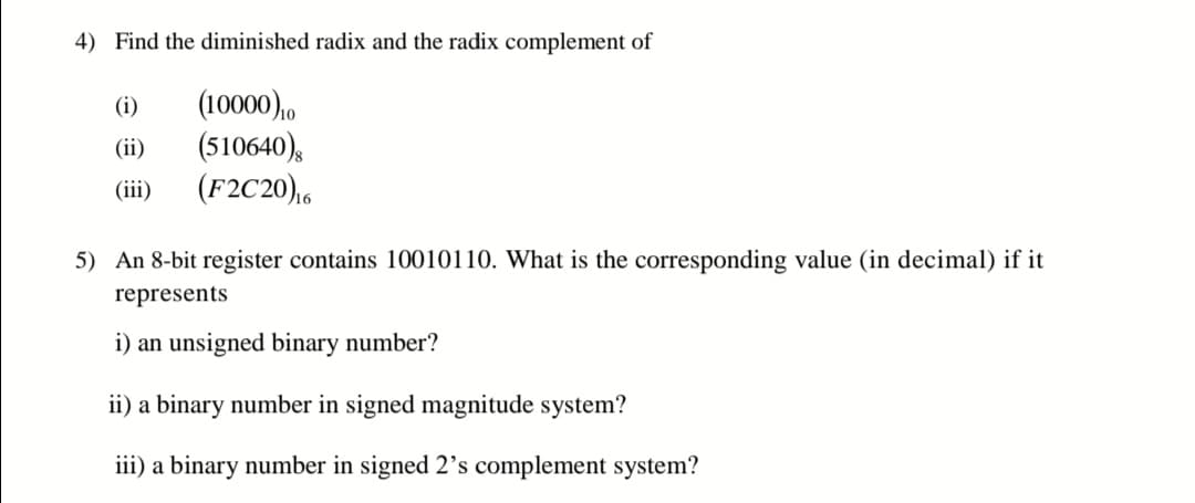
Transcribed Image Text:4) Find the diminished radix and the radix complement of
(10000),0
(510640),
(F2C20),,
(i)
(ii)
(iii)
5) An 8-bit register contains 10010110. What is the corresponding value (in decimal) if it
represents
i) an unsigned binary number?
ii) a binary number in signed magnitude system?
iii) a binary number in signed 2's complement system?
Expert Solution
This question has been solved!
Explore an expertly crafted, step-by-step solution for a thorough understanding of key concepts.

Step by step
Solved in 5 steps

Recommended textbooks for you

Delmar's Standard Textbook Of Electricity
Electrical Engineering
ISBN:
9781337900348
Author:
Stephen L. Herman
Publisher:
Cengage Learning
Delmar's Standard Textbook Of Electricity
Electrical Engineering
ISBN:
9781337900348
Author:
Stephen L. Herman
Publisher:
Cengage Learning