4. CMOS Logic Gate The PUN of a CMOS Logic Gate is shown below Vdd B-d 02 c 'Q3 B-das A-예- Q6 Q4 Q7 D Y (a) Determine Y from the PUN. Express your answer in Sum-of-Product form.
4. CMOS Logic Gate The PUN of a CMOS Logic Gate is shown below Vdd B-d 02 c 'Q3 B-das A-예- Q6 Q4 Q7 D Y (a) Determine Y from the PUN. Express your answer in Sum-of-Product form.

Chapter22: Sequence Control
Section: Chapter Questions
Problem 6SQ: Draw a symbol for a solid-state logic element AND.

Related questions
Question
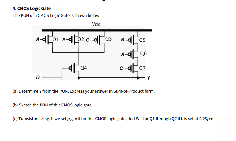
Transcribed Image Text:4. CMOS Logic Gate
The PUN of a CMOS Logic Gate is shown below
Vdd
Q1 B-
Q2 c -dPQ3
B-dCa5
Q6
D
Y
(a) Determine Y from the PUN. Express your answer in Sum-of-Product form.
(b) Sketch the PDN of this CMOS logic gate.
(c) Transistor sizing. If we set Peg = 5 for this CMOS logic gate, find W's for Q1 through Q7 if L is set at 0.25µm.
Expert Solution
This question has been solved!
Explore an expertly crafted, step-by-step solution for a thorough understanding of key concepts.

This is a popular solution!

Trending now
This is a popular solution!

Step by step
Solved in 2 steps with 2 images

Knowledge Booster


Learn more about
Need a deep-dive on the concept behind this application? Look no further. Learn more about this topic, electrical-engineering and related others by exploring similar questions and additional content below.Recommended textbooks for you