a) A logic circuit shown in Figure Q.3 has a 4-bit input A and B, three 4-bit wide 2:1 muxes, a 4-bit adder, a 4-bit output F, and a carry flag C. For the given Table Q.3, fill in the value of output F and carry flag C for the given value of A, B, S0, S1 and S2. 52 1001 FlagC 0011 Figure Q.3 Table Q.3 Elag C
a) A logic circuit shown in Figure Q.3 has a 4-bit input A and B, three 4-bit wide 2:1 muxes, a 4-bit adder, a 4-bit output F, and a carry flag C. For the given Table Q.3, fill in the value of output F and carry flag C for the given value of A, B, S0, S1 and S2. 52 1001 FlagC 0011 Figure Q.3 Table Q.3 Elag C

Chapter22: Sequence Control
Section: Chapter Questions
Problem 6SQ: Draw a symbol for a solid-state logic element AND.

Related questions
Question
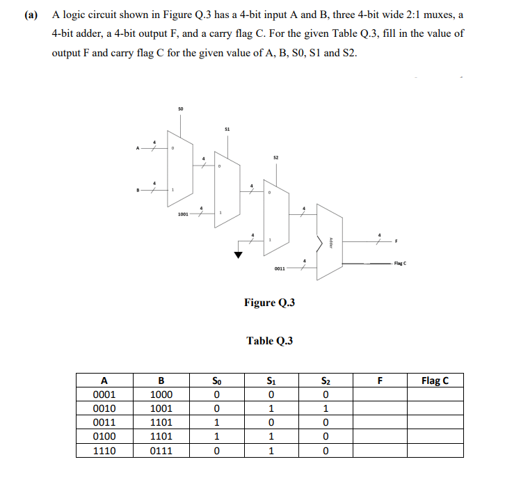
Transcribed Image Text:(a) A logic circuit shown in Figure Q.3 has a 4-bit input A and B, three 4-bit wide 2:1 muxes, a
4-bit adder, a 4-bit output F, and a carry flag C. For the given Table Q.3, fill in the value of
output F and carry flag C for the given value of A, B, S0, S1 and S2.
51
52
1001
Flag C
0011
Figure Q.3
Table Q.3
A
So
S1
S2
F
Flag C
0001
1000
0010
1001
1
1
0011
1101
0100
1101
1110
0111
1
Expert Solution
This question has been solved!
Explore an expertly crafted, step-by-step solution for a thorough understanding of key concepts.

Step by step
Solved in 6 steps with 6 images

Knowledge Booster


Learn more about
Need a deep-dive on the concept behind this application? Look no further. Learn more about this topic, electrical-engineering and related others by exploring similar questions and additional content below.Recommended textbooks for you