Given the following pullup circuit A-Design the pulldown circuitry B- What is the logic function implemented by this would be?
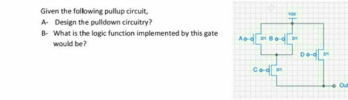
Q: For the logic circuit shown in the figure below, derive the Boolean expression of Y, simplify it,…
A: This is NAND, AND and NOR gate consist in the circuit. Find the expression of the y?
Q: 3.(a) Make a truth table for this given logic gate, as shown in the figure. Show the steps. What is…
A: “Since you have asked multiple questions, we will solve the first question for you. If you want any…
Q: ) Analyze the logic circuit in Figure Q5(c) and obtain the Boolean expression for Z. ii) Construct…
A:
Q: Analyze the logic circuits shown below in order to obtain the logic function for each circuit. Write…
A:
Q: For the logic circuit shown in the figure below, derive the Boolean expression of Y simplify it, and…
A: the output expression of the given logic is solved by following procedure So,output of NOR gate is…
Q: A B 2
A: The given data is as follows:-
Q: a) For the given logic circuit diagram write the program by using the gate level modeling. b) For…
A: In given question, different modeling are asked. As per bartleby expert policy, only one individual…
Q: We want to design a circuit to detect prime numbers. The input of the circuit is a 4-bit binary…
A:
Q: a) Explain the working of the circuit given in Figure 1 for inputs A = 0 and B = 0 and A = 1 and B =…
A: Given circuit consist of the BJT, when the Base of the BJT trigger its allow to pass the current…
Q: Determine the output expression of the below logic circuit. A B C F
A: Given, The logic circuit is,
Q: V dd Q1 Q2 Q5 Q3 A - Output Q4 Q6 B Write down the truth table for above logic gate with the ON /…
A:
Q: Distinguish between Half Adder and Full Adder
A: Adder: Adder is digital circuit that performs addition operation of numbers. In computers adders…
Q: Q2. Minimize the combinational logic circuit in the following figure using Karnaugh's map only.…
A:
Q: 2. Realize the following function F(A_B.C.D) =E(1,2,5,6,7,11) using a (a) 4-to-1 multiplexer, and…
A:
Q: Figure Q.4 (a) shows a combinational logic circuit with output, Z and Table Q.4(a) depicts the delay…
A: According to the question, for the figure shown below We need to find the critical path and…
Q: Draw a logic diagram using only two-input NAND gates to implement the following expression: (AB +…
A:
Q: a. Construct a Karnaugh map for the logic function D=ABC+ A ¯ BC+AB C ¯ +BC b. Find the minimum SOP…
A: A: The k-map for the given function in SOP form is shown below: B: From the K-map the simplified…
Q: 4. For the NOR gate function shown below A Da B. Do a) Write the switching expression for the…
A:
Q: (b)For the logic circuit below what is F=? A
A: First we will identify the given gate and than we will write output equation of that gate and than…
Q: Draw the logic diagram of a full adder circuit. Show the addition off 111 and 110 using cascaded…
A: According to the question, we need to draw the logic diagram of a full adder circuit. Show the…
Q: F a) Write the switching expression for the output, F(A,B,C,D) b) Simplify this switching function…
A: To simplify output, we will follow outputs from each gates and so on we can conclude final output F.…
Q: (b) Write the Boolean Expression from the given logic circuit in Figure Q5 (B). AD B DC Figure Q5…
A: The solution is as follows.
Q: Implement the following logic function using only 3-8 decoders and logic gates. ?(?,?,?,?)=…
A:
Q: "For the logic circuit chown below FA F F=AB'+AB O E-A+B O F-AB F-A+B O
A: In this answer we will try to find the value of F as explained below.
Q: Design the logic circuit that performs the logic function below. B’(AB+C’)+A
A:
Q: NOR IMPLEMENTATION Given Boolean Function: (AB +B'C')' Instruction: A. Construct the truth table. B.…
A: Given- F= AB+B'C'' To find- A. Truth table =? B. Logic circuit diagram using gates =? C. Logic…
Q: logic function defined by the truth table of Figure below. b. What is the minimum expression for…
A:
Q: Q2: Draw a Flowchart to perform the function (G) for the logic circuit shown below, that outputs are…
A: Given
Q: 2. 2-to-1-Line Multiplexer Design a. Write the Condensed Truth Table of a 2-to-1 line Multiplexer b.…
A:
Q: Design the logic circuit that drives the LED of one of the segments in a 7-segment display
A: 7-Segment Display: 7-Segment Display is defined as the form of electronic display,used to display…
Q: a. Formulate Carry Look-ahead Generator. b. Design the circuit of Carry Look-ahead Generator. c.…
A: 4 bit adder with carry look ahead generator This adder reduces the carry delay by reducing the…
Q: Find a logic diagram that corresponds to the VHDL structural description in below figure. Note that…
A: In the structural model, the hardware is described as the interconnection of modules. Any instance…
Q: Design the circuit of OR gate with three input using simple logic module ?
A: Given that: The number of inputs =3 Output =1
Q: Draw the combinational logic circuit diagram by using the equation (ab’ . (a + c))’ + a’b . (a +b’…
A:
Q: 3.5 Design a logic circuit from the following switch function using Boolean theory using only NOR…
A:
Q: Draw the logic circuit for the following function: F = D + BC + (D + C )(A + C)
A:
Q: Design a logic cirčuit with four inputs and if the input patterns have odd number of zeros. a) Write…
A:
Q: Design a logic circuit to implement a Mealy type sequence detector to detect the input sequence 11
A: sequence detector to detect the input sequence 011: State diagram: State table: Boolean…
Q: Consider the logic diagram and the timing diagram of the inputs X and Y graph below and answer the…
A: It is combination of NOT gate and AND gate Output z is fed back to NOT gate as feedback
Q: What are logic circuits, what are the similarities and differences between asynchronous numbers and…
A: 1. What are logic circuits? The logic circuit is a circuit whose output depends on the input given…
Q: A В Q1 Q2
A: Given diagram
Q: Q (A, B, C) = A' .B'. C +A' .B. C + A.B.C' + A.B.C Obtain the simplified function with the…
A:
Q: Which of the following logic operation can be performed using only “NOR” gate ? AND, OR and NOT…
A: The explanation is as follows.
Q: Draw the logic diagram to implement the following Boolean expression using only NAND gates. Y=…
A:
Q: Draw the circuit diagram of a full adder by using two blocks of half-adders and one basic logic…
A:
Q: - Implement a logic circuit to verify the following logic function: F= E 1,2,3,4,5,7,8,12,13|| The…
A: Given Function F = Em ( 1,2,3,4,5,7,8,12,13) the given function is in SOP form let the variables are…
Q: Type the structural VHDL code that describes the expression F = AB' + A' B. %3D Assume that the VHDL…
A: We need to type the VHDL code that describes the expression F=AB'+A'B. We need to use Exps as the…
Q: Draw the equivalent ladder diagram for the following combinational logic function using light…
A:
Q: n equation in reduced SOP form, is F=AB+B'C+A'C'. I need to draw a logic circuit F using NOT/AND/OR…
A: We are authorized to answer one question at a time, since you have not mentioned which question you…
Step by step
Solved in 2 steps with 2 images
- Design a 4-bit synchronous binary upcounter using T flip-flops. Draw only the logic diagram. Please show the process.Use Digital Logic Simulator Fill-in the blank boxes with the correct LOGIC GATE/ Full/Half Adder.Provide a detailed report on the combinational logic circuits below. 1. Magnitude Comparators a. What are magnitude comparators? b. How does it work? c. Applications of magnitude comparators.
- An equation in reduced SOP form, is F=AB+B'C+A'C'. I need to draw a logic circuit F using NOT/AND/OR and logoc circuit F using all NAND gates. Thank you for the help. I understood the previous types of gates but I am confused on how to draw these circuits.a) Static logic circuit is a design methodology in integrated circuit design where there is at all times some mechanism to drive the output either high or low. A static CMOS gate is a combination of two networks, called the pull-up network (PUN) and the pull- down network (PDN). With the back ground stated , explain in your own words the principle of PUN and PDN with respect to static logic circuit formationDesign a digital logic circuit using only NAND gates for the logic expressiongiven by: F=A.(B +C)
- Draw the combinational logic circuit diagram by using the equation (ab’ . (a + c))’ + a’b . (a +b’ + c’)’Given the state diagram below, generate the (a)state table, (b)state equations, (c)output equation and (d) flip-flop inputs. Afterwhich, draw the (e)equivalent logic diagram using JK flip-flop.Create the logic diagram of the two bits full adder
- Draw a 14 ic chip wiring diagram with labeled switches(A, B, C) of a 3 input of this logic diagram.Find a logic diagram that corresponds to the VHDL structural description in below figure. Note that complemented inputs are not availablechoose the correct answer Logic gates from which of the following logic families are suitable for VLSI circuits? a. MOS b. ECL c. CMOS d. TTL