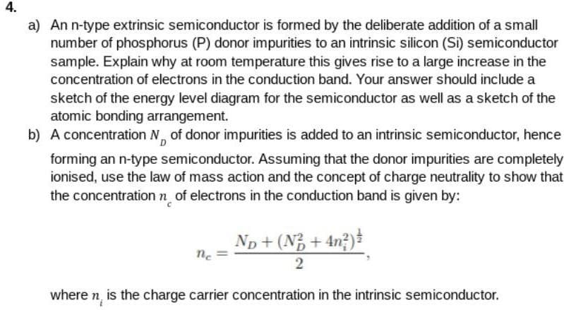
a) An n-type extrinsic semiconductor is formed by the deliberate addition of a small number of phosphorus (P) donor impurities to an intrinsic silicon (Si) semiconductor sample. Explain why at room temperature this gives rise to a large increase in the concentration of electrons in the conduction band. Your answer should include a sketch of the energy level diagram for the semiconductor as well as a sketch of the atomic bonding arrangement. b) A concentration N of donor impurities is added to an intrinsic semiconductor, hence forming an n-type semiconductor. Assuming that the donor impurities are completely ionised, use the law of mass action and the concept of charge neutrality to show that the concentration n of electrons in the conduction band is given by: ne N₁ + (№² +4n²) 2 where n, is the charge carrier concentration in the intrinsic semiconductor.
a) An n-type extrinsic semiconductor is formed by the deliberate addition of a small number of phosphorus (P) donor impurities to an intrinsic silicon (Si) semiconductor sample. Explain why at room temperature this gives rise to a large increase in the concentration of electrons in the conduction band. Your answer should include a sketch of the energy level diagram for the semiconductor as well as a sketch of the atomic bonding arrangement. b) A concentration N of donor impurities is added to an intrinsic semiconductor, hence forming an n-type semiconductor. Assuming that the donor impurities are completely ionised, use the law of mass action and the concept of charge neutrality to show that the concentration n of electrons in the conduction band is given by: ne N₁ + (№² +4n²) 2 where n, is the charge carrier concentration in the intrinsic semiconductor.
Power System Analysis and Design (MindTap Course List)
6th Edition
ISBN:9781305632134
Author:J. Duncan Glover, Thomas Overbye, Mulukutla S. Sarma
Publisher:J. Duncan Glover, Thomas Overbye, Mulukutla S. Sarma
Chapter4: Transmission Line Parameters
Section: Chapter Questions
Problem 4.2P: The temperature dependence of resistance is also quantified by the relation R2=R1[ 1+(T2T1) ] where...
Related questions
Question
I2

Transcribed Image Text:4.
a) An n-type extrinsic semiconductor is formed by the deliberate addition of a small
number of phosphorus (P) donor impurities to an intrinsic silicon (Si) semiconductor
sample. Explain why at room temperature this gives rise to a large increase in the
concentration of electrons in the conduction band. Your answer should include a
sketch of the energy level diagram for the semiconductor as well as a sketch of the
atomic bonding arrangement.
b) A concentration N, of donor impurities is added to an intrinsic semiconductor, hence
forming an n-type semiconductor. Assuming that the donor impurities are completely
ionised, use the law of mass action and the concept of charge neutrality to show that
the concentration of electrons in the conduction band is given by:
ne
N₂ + (№² +4n²) ³
2
where n is the charge carrier concentration in the intrinsic semiconductor.
Expert Solution
This question has been solved!
Explore an expertly crafted, step-by-step solution for a thorough understanding of key concepts.
Step by step
Solved in 3 steps with 2 images

Knowledge Booster
Learn more about
Need a deep-dive on the concept behind this application? Look no further. Learn more about this topic, electrical-engineering and related others by exploring similar questions and additional content below.Recommended textbooks for you

Power System Analysis and Design (MindTap Course …
Electrical Engineering
ISBN:
9781305632134
Author:
J. Duncan Glover, Thomas Overbye, Mulukutla S. Sarma
Publisher:
Cengage Learning

Power System Analysis and Design (MindTap Course …
Electrical Engineering
ISBN:
9781305632134
Author:
J. Duncan Glover, Thomas Overbye, Mulukutla S. Sarma
Publisher:
Cengage Learning